-
It’s Time for an Upgrade: CMOS ADC with Chopper
It’s Time for an Upgrade: CMOS ADC with Chopper
Thomas Neu
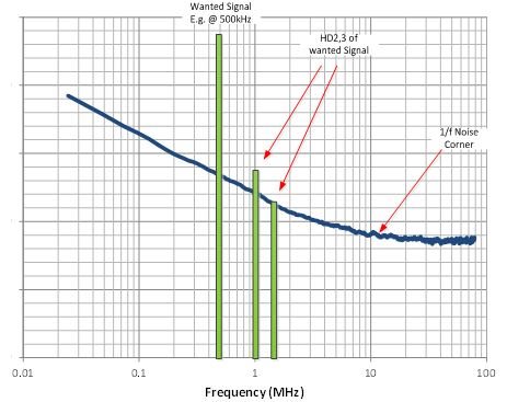
Until recently, industrial applications such as precision motor control or plasma etchers couldn’t take full advantage of modern high-speed data converters. Because these systems monitor a small input signal at a few hundred kilohertz and its even smaller harmonics, they are very sensitive to the 1/f noise or flicker noise of the high-speed data converter (see Figure 1).
 Figure 1 Wanted Signal and Its
Harmonics in the Presence of 1/F Noise
Figure 1 Wanted Signal and Its
Harmonics in the Presence of 1/F NoiseUnfortunately for these applications, high-speed analog-to-digital converters (ADCs) are moving toward finer, more advanced process geometries. The 1/f noise corner of bipolar transistors is around 100kHz; for complementary metal-oxide semiconductor (CMOS) transistors (depending on actual process geometry), it is around 10MHz or greater. So the 1/f noise corner of CMOS ADCs is significantly worse/higher compared to bipolar transistors and directly overlaps with the very-low-frequency input range used in many industrial applications.
You can overcome this limitation, however, with a clever but very effective design feature called a chopper front end. Many designers of industrial applications are already finding the new ADC3k family because it is outfitted with an internal chopper front end.
How the Chopper Feature Works
The name “chopper” originated many years ago from a circuit that converted a DC voltage input into a variable DC output voltage. In modern electronics, all kinds of different switching circuits that shift unwanted noise around are labeled as chopper circuits.
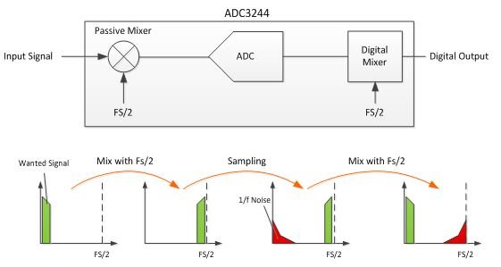
In the ADC3k, the key idea of the chopper is to transfer the 1/f noise to a different frequency range, away from the input signal close to DC. The chopper circuit basically consists of a passive mixer (operating at half the sampling rate) plus some digital logic. Instead of shifting the 1/f noise away, the passive mixer basically inverts the input-frequency spectrum prior to the sampling instant. Thus, it transfers the low-frequency input signal to the opposite end of the Nyquist zone of the ADC. After sampling, a digital mixer inverts the spectrum once more, transforming everything back to its original location as illustrated in Figure 2.
 Figure 2 Chopper Implementation Details
of the ADC3244
Figure 2 Chopper Implementation Details
of the ADC3244The Chopper in Action
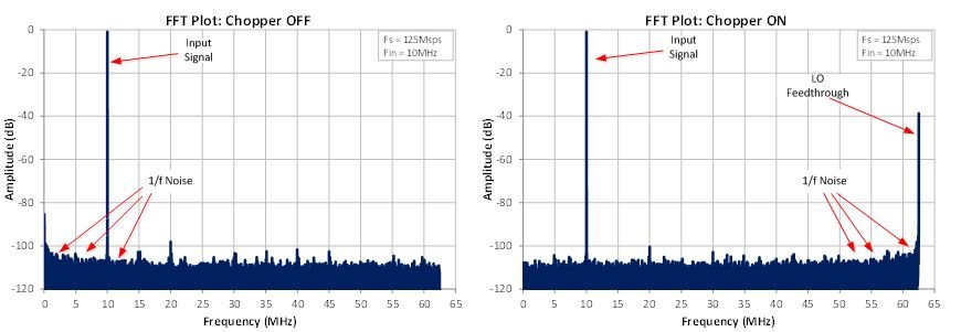
The fast Fourier transform (FFT) spectrum with chopper disabled (Figure 3, left) shows the input signal along with the 1/f noise close to DC. After enabling the chopper feature, the input signal remains unchanged at 10MHz, while the low-frequency 1/f noise is now shifted to the opposite side of the Nyquist zone at Fs/2.
The chopper feature does bring one additional, unwanted byproduct. As you can see in the FFT plot on the right side of Figure 3, the passive mixer also generates a large spur at Fs/2. This is known as the local oscillator (LO) feedthrough, where the LO input is coupling into the output spectrum. This spur, along with the unwanted 1/f noise, is far away from the frequency range of interest; however, you can remove both with a digital filter.
 Figure 3 A 10MHz Input Signal with the
Chopper Disabled (Left) and Enabled (Right)
Figure 3 A 10MHz Input Signal with the
Chopper Disabled (Left) and Enabled (Right)Industrial applications requiring very good noise performance in the low-frequency region could traditionally only use bipolar transistor-based high-speed ADCs that provide the lowest 1/f noise profiles. A chopper is a very innovative feature that eliminates this inherent disadvantage of CMOS converters. Adding the chopper feature allows system designers to take advantage of modern, much lower-power CMOS data converters.
How would you like to use a chopper-stabilized ADC in your next design? Let us know with a comment below.
Additional Resources
- Learn more about TI’s high-speed industrial ADCs.
- Ask questions, share knowledge and explore ideas on the TI E2E™ Community High Speed Data Converters forum.
- Read the ADC3244 data sheet.
- Learn about TI’s data converter portfolio and find technical resources.
IMPORTANT NOTICE AND DISCLAIMER
TI PROVIDES TECHNICAL AND RELIABILITY DATA (INCLUDING DATASHEETS), DESIGN RESOURCES (INCLUDING REFERENCE DESIGNS), APPLICATION OR OTHER DESIGN ADVICE, WEB TOOLS, SAFETY INFORMATION, AND OTHER RESOURCES “AS IS” AND WITH ALL FAULTS, AND DISCLAIMS ALL WARRANTIES, EXPRESS AND IMPLIED, INCLUDING WITHOUT LIMITATION ANY IMPLIED WARRANTIES OF MERCHANTABILITY, FITNESS FOR A PARTICULAR PURPOSE OR NON-INFRINGEMENT OF THIRD PARTY INTELLECTUAL PROPERTY RIGHTS.
These resources are intended for skilled developers designing with TI products. You are solely responsible for (1) selecting the appropriate TI products for your application, (2) designing, validating and testing your application, and (3) ensuring your application meets applicable standards, and any other safety, security, or other requirements. These resources are subject to change without notice. TI grants you permission to use these resources only for development of an application that uses the TI products described in the resource. Other reproduction and display of these resources is prohibited. No license is granted to any other TI intellectual property right or to any third party intellectual property right. TI disclaims responsibility for, and you will fully indemnify TI and its representatives against, any claims, damages, costs, losses, and liabilities arising out of your use of these resources.
TI’s products are provided subject to TI’s Terms of Sale (www.ti.com/legal/termsofsale.html) or other applicable terms available either on ti.com or provided in conjunction with such TI products. TI’s provision of these resources does not expand or otherwise alter TI’s applicable warranties or warranty disclaimers for TI products.
Mailing Address: Texas Instruments, Post Office Box 655303, Dallas, Texas 75265
Copyright © 2023, Texas Instruments Incorporated