SSZTC40 october 2015
There are applications that require loose output regulation and current less than 20mA. For such applications, a linear regulator built with discrete components is a cost-effective solution (Figure 1). For applications with tight output regulation and requires more current, a high performance LDO can be used.
 Figure 1 A simple series voltage
regulator.
Figure 1 A simple series voltage
regulator.There are two design challenges related to the circuit shown in Figure 1. The first challenge is to regulate output voltage, and the second challenge is to survive a short-circuit event. In this post, I will discuss how to design a robust linear regulator with discrete components.
Here is an example used to power a microcontroller:
- Input range: 8.4V to 12.6V.
- Output range: 1.71V to 3.7V.
- Maximum load current: Io_max = 20mA.
Bipolar NPN Transistor Selection
The NPN bipolar transistor, Q1, is the most important component. I selected this device first. The transistor should meet the following requirements:
- The collector-to-emitter and base-to-emitter breakdown voltage should be higher than the maximum input voltage, Vin_max.
- The maximum allowable collector current should be greater than the maximum load current, Io_max.
Besides these two basic requirements, it is a good idea to use a component with alternative packages. When it comes to power dissipation, having this flexibility will ease the design process later. For this application, I selected a NPN transistor with alternative packages and different power ratings.
Here are the key characteristic of the NPN transistor I used.
With IC = 50mA:
the DC current gain, hFE = 60;
the maximum collector-emitter saturation voltage VCEsat = 300mV;
the maximum base-emitter saturation voltage VBEsat = 950mV.
Zener Diode, Dz Selection
The output voltage is the reverse zener voltage, VZ, subtracting the transistor base-to-emitter voltage, VBE. Thus, the minimum reverse zener voltage meets the following requirement (Equation 1):
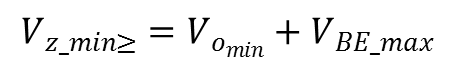
With Vo_min = 1.71V and VBE_max= 0.95V, Vz_min should be greater than 2.65V.
For this application, I used a test condition of IZT = 1mA and selected a zener diode with the following characteristics:
With reverse current of IZT = 1mA, the minimum reverse voltage, VZ_min = 2.7V.
With reverse current of IZT = 5mA, the maximum reverse voltage, VZ_max = 3.8V.
Base Pull-up Resistor, RB
The resistor, RB, provides current for both the zener diode and transistor base. It should provide sufficient current over the operating conditions. The zener diode reverse current, IZ, should be greater than 1mA, as I discussed in the “zener diode, Dz selection” section. Equation 2 estimates the maximum base current required for operation:
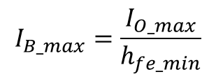
where Hfe_min = 60. Thus, IB_max ≈ 0.333mA.
Equation 3 calculates the value of RB. I used a resistor with 1% tolerance.
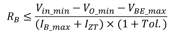
Thus, RB should be less than 4.26kΩ. I used a resistor with a standard 4.22kΩ value.
Adding a dummy load resistor for output regulation
Output voltage is at its maximum when the load current is zero. With 1mA ≤IZT ≤ 5mA, the maximum VZ is 3.8. . VBE(on) should be greater than 0.1V so that the output of the regulator meets the requirement. I added a dummy load resistor to draw a collector current for a no-load condition.
Figure 2 shows VBE(on) as a function of the collector current, IC. With IC = 0.1mA, VBE(on) is greater than 0.3V.
 Figure 2 Base-emitter on voltage versus
collector current
Figure 2 Base-emitter on voltage versus
collector currentEquation 4 calculates the dummy resistor:
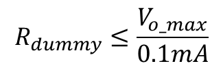
I added a 36kΩ resistor to the circuit, as shown in Figure 3.
 Figure 3 Series voltage regulator with
a dummy load resistor
Figure 3 Series voltage regulator with
a dummy load resistorCurrent Limiting for a Short-circuit Event
Shorting the output of the circuit shown in Figure 3 to ground will result in high collector current. A PSPICE simulation result shows that the collector current could be as high as 190mA; see Figure 4.
 Figure 4 Short-circuit simulation
result
Figure 4 Short-circuit simulation
resultThe power dissipation on the transistor, Q1, is 2.4W. No package can handle this power dissipation.
To limit the short-circuit current, I added a resistor, RC, from VIN to the collector of the transistor, Q1, as shown in Figure 5.
 Figure 5 Series voltage regulator with
a current-limiting resistor
Figure 5 Series voltage regulator with
a current-limiting resistorThe resistor, RC, will meet the output-regulation requirement and is capable of dissipating power during short-circuit events. I calculates the value of RC:
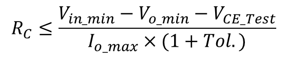
VCE_Test is the collector-emitter voltage used in Figure 1. I selected a 5% tolerance resistor for RC. Using Equation 5, RC should be less than 271Ω. With this estimated value, Equation 6 calculates the worst-case power dissipation on RC in a short-circuit event:
The power dissipation is about 0.56W. I selected a 1W, 270Ω power resistor. For applications with much higher short-circuit power dissipation on RC, you can put multiple resistors in series to share the power.
Component Stress Analysis
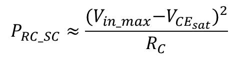
For the resistor, RC, the worst-case power dissipation occurs in a short-circuit event with maximum input. Using Equation 6, the maximum power dissipation is 0.59W.
For the transistor, Q1, the worst-case power dissipation is not during short-circuit event because of the current-limiting resistor, RC. The power dissipation on Q1 during normal operation is a function of the collector current, as shown in Equation 7:
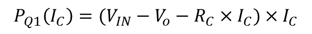
The worst case happens when:
VIN = VIN_max
VO = VO_min
IC = (VIN_max – VO_min)/(2×RC)
Thus, the maximum power dissipation on Q1 is (VIN_max – VO_min)2/(4×RC). For this example, it is 110mW. I selected a small-outline-transistor, SOT23 package rated for 350mW.
For the maximum power dissipation on RB, the worst case occurs during a short-circuit event with maximum input. The voltage across RB is the input voltage subtracting the VBE(sat). The maximum power dissipation is estimated as 38mW.
In this post, I described the design guidelines for a robust, low-cost linear regulator with discrete components. This design process proves that integrated linear regulator from Texas Instruments provides much better output regulation and complete protections again over-voltage, short-circuit and over temperature.
Additional Resources
- Read more Power Tips.
- View Power Tips videos: https://training.ti.com/power-tips-training-series
- Watch this overview of NPN voltage regulators