SSZTCK9 june 2015 LM2771 , LM2775

|

|
As a designer, choosing the right power supply topology is essential. Making the wrong choice means angry customers and lost time and money. When looking at voltage regulation, the usual trade-offs of size, efficiency, accuracy and voltage ripple are important. But so too is the topology of the solution. Should it be an inductor-based converter, linear regulator (LDO) or charge pump? While charge pump ICs aren’t the optimal solution for every design, they do possess several advantages over an inductive converter and increased efficiency over an LDO. Let’s explore a few reasons to consider a charge pump.
Charge Pumps Are Simpler, Smaller and Come in the Same Building-block Capabilities as Inductive DC/DC Converters
A charge pump converter provides an easy-to-use, small solution size, with ruggedness not found in inductive DC/DC converters. Charge pumps also can be found in boost, buck and inverting flavors, just like their magnetic brethren, without the inductor cost, height and printed circuit board (PCB) area requirements.
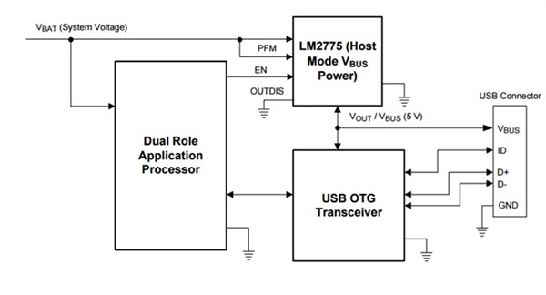
If you compare a charge pump-based buck regulator against an inductive solution, you can eliminate the inductor. The trade-off is about 10-20% lower efficiency than an inductive buck, but the charge pump saves space on your board. Charge pump circuits also are great for inverting an input voltage and for boosting. See Figure 1 for an example of how to use a boost charge pump.
 Figure 1 The LM2775
Is Often Used for Universal Serial Bus (USB) On-the-Go (OTG)/Mobile HDMI
Applications
Figure 1 The LM2775
Is Often Used for Universal Serial Bus (USB) On-the-Go (OTG)/Mobile HDMI
ApplicationsIn Figure 1, the regulated 5V output mode on the LM2775 (a switched capacitor 5V boost converter) is often used for a USB OTG/mobile HDMI application. You can enable/disable the LM2775 by applying a logic signal on only the EN pin, while grounding the OUTDIS pin. Depending on the USB/HDMI mode of the application, you could also enable the LM2775 to drive the power bus line (host), or disable it to put its output in high impedance, allowing an external supply to drive the bus line (slave). In addition to the high-impedance back-drive protection, the output current-limit protection is 200mA (typical), well within USB OTG and HDMI requirements.
Charge Pumps Offer Greater Efficiency than LDOs
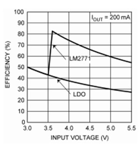
Charge pump regulators have approximately 20% greater efficiency over an LDO, while only increasing the solution size by adding two small ceramic capacitors. Figure 2 shows an example of where a charge pump could be used versus an LDO, as long as output ripple is not a huge design issue. In this situation, regulation is achieved by current control through the input-connected switches or pulse-frequency modulation. Most devices of this nature also include a low-impedance pass mode for when the input to output ratio approaches 1. This gain and efficiency and switch to pass mode is highlighted in the efficiency curve of the LM2771, low-ripple 250mA switched-capacitor step-down DC/DC converter, regulating the output voltage at 1.5V. In this application, the curve highlights that a 30% efficiency gain is possible by using a regulated charge pump circuit (Figure 2).
 Figure 2 The Curve Highlights a 30% Efficiency Gain Using a Regulated Charge Pump versus a LDO
While a charge pump may not be the optimal solution for every DC/DC converter design, it does provide several advantages over inductive converters, including lower cost and smaller PCB size. A charge pump IC also provides increased efficiency over an LDO. To learn more about specific situations for which charge pumps are ideal, check out my next blog coming up in July.
Additional Resources:
- Browse product tables for: