Clamp Diodes: a One-way Street
C. Ryan Land
“Am I allowed to have an input signal when VCC = 0 V?”
“What happens if the input or output voltage goes below GND?”
Customers ask these questions quite frequently – and for good reasons. Many standard logic datasheets don’t specify explicitly if conditions are allowed where inputs go above VCC or below ground (GND). The devices themselves have few (if any) performance characteristics in the datasheet at those fringe voltages.
One of the most important features of most TI devices is the presence of electrostatic discharge (ESD) protection. In fact, in some devices, ESD protection circuitry takes up most of the space on the die. Typically, an ESD circuit includes a diode that channels excess current to GND (through reverse breakdown) or VCC (through forward biasing) when the input voltage approaches unsafe levels. The intent is to protect against damaging conditions in the internal circuitry.
However, the ESD diodes can have some unintended effects. For example, if there is an input diode going from the input to VCC, an input voltage at VCC = 0 will cause current to flow through the device to the VCC pin. Likewise, a diode from GND to the input will cause current to flow from GND to the input when the input reaches a certain level below GND.
So how do we know when the input diodes are present, and how can we protect against negative effects?
The absolute maximum ratings table (Figure 1) holds the answers.
 Figure 1 Sample Absolute Maximum
Ratings Table
Figure 1 Sample Absolute Maximum
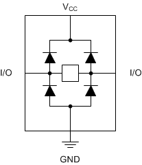
Ratings TableOn this analog switch, we can see that a voltage on the I/O pins is not allowed to be higher than VCC, or less than -0.5V. Therefore, we can conclude that there is a diode to VCC and a diode from GND on each I/O port of the device.
 Figure 2 ESD Diode Structure of Device
with Absolute Max Table Similar to Table 1
Figure 2 ESD Diode Structure of Device
with Absolute Max Table Similar to Table 1Figure 3 offers another example where the absolute maximum rating is structured a bit differently.
 Figure 3 Sample Absolute Maximum
Ratings table with different limits on inputs vs. outputs
Figure 3 Sample Absolute Maximum
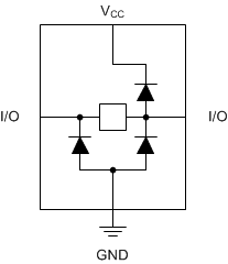
Ratings table with different limits on inputs vs. outputsWe can see here that the diode is present from GND to both the input and output, and the ESD diode to VCC is present at the output. When the device is in a high or low state, there is a risk of conducting current through the VCC diode. This device has a special feature called a high-impedance state that prevents current backflow through the diode. It also has protection circuitry for when VCC = 0, called IOFF.
However, from the VCC + 0.5V statement, we know there is a diode going from the output to VCC, and there is protection circuitry to prevent issues in certain configurations.
 Figure 4 ESD Diode Structure for Device
with Absolute Maximum Ratings Similar to Figure 3
Figure 4 ESD Diode Structure for Device
with Absolute Maximum Ratings Similar to Figure 3But what are the limits? The specs IIK and IOK describe the current limits into the device (positive values) and out of the device (negative values) through ESD diodes. Consider the first case (Figure 5), where we had two GND diodes.
 Figure 5 Sample Ratings for Clamp
Currents in Absolute Maximum Ratings
Figure 5 Sample Ratings for Clamp
Currents in Absolute Maximum RatingsThe current in the GND diode is limited to 50mA. For the second case with the VCC diode, the “output clamp current” would have a +/- symbol, indicating that current can flow in both directions (into the VCC diode or out of the GND diode).
It is best to avoid situations where ESD diodes can turn on. Most data sheets specify an exception to the input and output voltage rules – so if you limit the diode clamp current with a series resistor on the input or output, your device will be at much less risk of damage.