SSZTCQ4 may 2015 TPS54260 , TPS54620
ADVANCE INFORMATION
Selecting the output capacitance in a buck converter is often based on the level of output-ripple voltage required. In many cases, the calculated capacitance may be rather small, allowing the use of only a single ceramic capacitor. Additionally, since ceramic capacitors have very low equivalent series resistance (ESR), their contribution to output ripple will be minimal. This is great, because it keeps costs low, so less capacitance is better.
But what if, after moving forward with your design, you discover during testing that a load transient is causing the output voltage to fall to an unacceptably low level? In this case, the only solution is to load up the output with more capacitance, forcing a new printed circuit board (PCB) layout.
I have a simple calculation that can prevent this kind of disaster.
 Figure 1 TPS54620 Synchronous Buck Converter
with Ceramic Output Capacitors
Figure 1 TPS54620 Synchronous Buck Converter
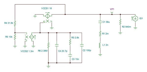
with Ceramic Output CapacitorsFigure 1 details an updated design with significantly more output capacitance. And to really understand what’s going on with the load-transient performance, I created the simulation model shown in Figure 2. I used this model to plot the open- and closed-loop output impedances and loop gain (or the converter’s bandwidth). The open-loop output impedance is simply the impedance looking into the output of the converter with feedback disabled. Since this design uses current-mode control, the inductor acts as a constant current source, and does not show up in the impedance plots. However, if this design had used voltage-mode control, the open-loop output impedance plot would have had a peak at the L-C resonant frequency.
The inductor’s impact is not negligible. A smaller inductance value allows the converter to increase its output current faster during a transient and should not be sized so large as to be slower than the bandwidth. The open-loop output impedance plot in Figure 2 is modeled as a single 58µF output capacitor in series with a small ESR and lead inductance. The effective output capacitance for two 47µF 6.3V capacitors with a 3.3VDC bias is 58µF. This plot looks capacitive with a -1 slope until it goes inductive above 500KHz.
 Figure 2 TPS54260 Simulation Model Showing
Closed-loop Output Impedance
Figure 2 TPS54260 Simulation Model Showing
Closed-loop Output ImpedanceThe closed-loop output impedance is the open-loop impedance divided by one plus the loop gain. The bandwidth of the converter is where the loop gain is equal to one. Above this frequency, the feedback offers little benefit to the output impedance, since the open- and closed-loop plots converge. Below the converter’s bandwidth, the large gain in the feedback loop decreases the effective output impedance. The peak of the closed-loop impedance closely correlates with the loop bandwidth. This is important because the change seen in the output voltage from a load transient is equal to this impedance times the load step. Since this impedance is nearly the same magnitude as the output capacitor’s impedance at the converter’s bandwidth, you can use this to approximate a load-step response.
 Figure 3 Simulation Shows That the
Closed-loop Output Impedance Reaches a Maximum near the Loop Bandwidth
Frequency
 Figure 4 Circuit Test of a 1.75A
Load Transient Results in an Output-voltage Change of 115mV
Figure 4 Circuit Test of a 1.75A
Load Transient Results in an Output-voltage Change of 115mVThe impedance of a capacitor is Z = 1 / (2π × f × C), so if you set this equal to ΔVout/ΔItran, you get the load-step approximation shown in Equation Figure 1:
 Figure 5 (1)
Figure 4 shows a lab test of a 1.75A load step and a corresponding 115mV output-voltage droop. Equation Figure 1, using the measured 38KHz bandwidth, estimates 126 mV.
Equation Figure 1 can provide a reasonable estimate of the ceramic output capacitance necessary for a load-current transient. In many cases, this calculated capacitance value can be significantly larger than that required for a low steady-state ripple voltage. You only need a good estimate of the converter’s bandwidth. Keep in mind that a capacitor with a high ESR (or using mixed capacitor types) may increase the expected voltage, so extra care (or simulations) may be necessary.
Additional Resources
- Check out TI’s Power Tips blog series on Power House.