SSZTCU9 February 2024 UCC28C50
The many virtues of flyback converters include being the lowest-cost isolated power converter, easily supplying multiple output voltages, a simple primary-side controller and power delivery of up to 300W. Flyback converters are used in many offline applications from televisions to phone chargers as well telecommunications and industrial applications. Their basic operation can appear intimidating and the design choices are many, especially for those who have not designed one before. Let’s look at some of the key design considerations for a 53 VDC to 12V at 5A continuous-conduction mode (CCM) flyback.
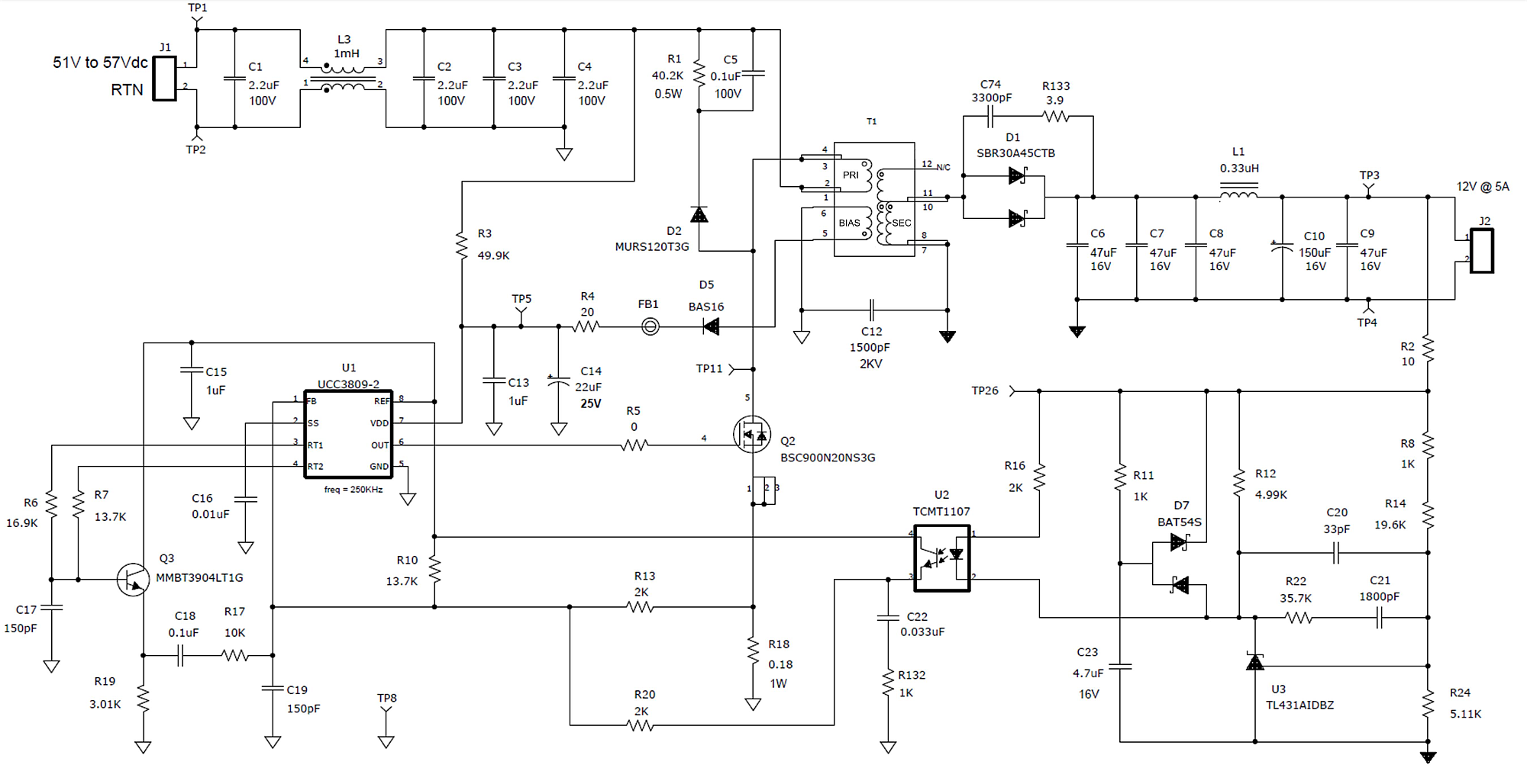
Figure 1 shows a detailed 60W flyback schematic, operating at 250 kHz. When FET Q2 turns on, the input voltage is applied across the transformer’s primary winding. Current in the winding now ramps up, allowing energy to be stored in the transformer. Since output rectifier D1 is reverse-biased, current flow to the output is blocked. When Q2 turns off, primary current is interrupted, forcing the winding’s voltage polarities to reverse. Current now flows out of the secondary winding, reversing the polarity of the winding voltage with the dot-voltage positive. D1 conducts, delivering current to the output load and recharging the output capacitors.
 Figure 1 60 W CCM flyback converter
schematic.
Figure 1 60 W CCM flyback converter
schematic.Additional transformer windings can be added, or even stacked on top of other windings, to obtain additional outputs. However, the more outputs added, the worse their regulation will be. This because of the imperfect magnetic flux linkages between the windings and the core (coupling) and the physical separation of the windings, creating leakage inductance. Leakage inductance acts as stray inductance in series with the primary and the output windings. This creates an unintended voltage drop in series with the windings, effectively decreasing output voltage regulation accuracy. A general rule of thumb is to expect non-regulated outputs to vary +/–5 to 10%, over cross-loading, with a properly wound transformer. Additionally, a heavy-loaded regulated output can cause a large increase in an unloaded secondary output’s voltage by peak-detecting leakage-induced voltage spikes. In this case, a preload or soft clamp can help limit the voltage.
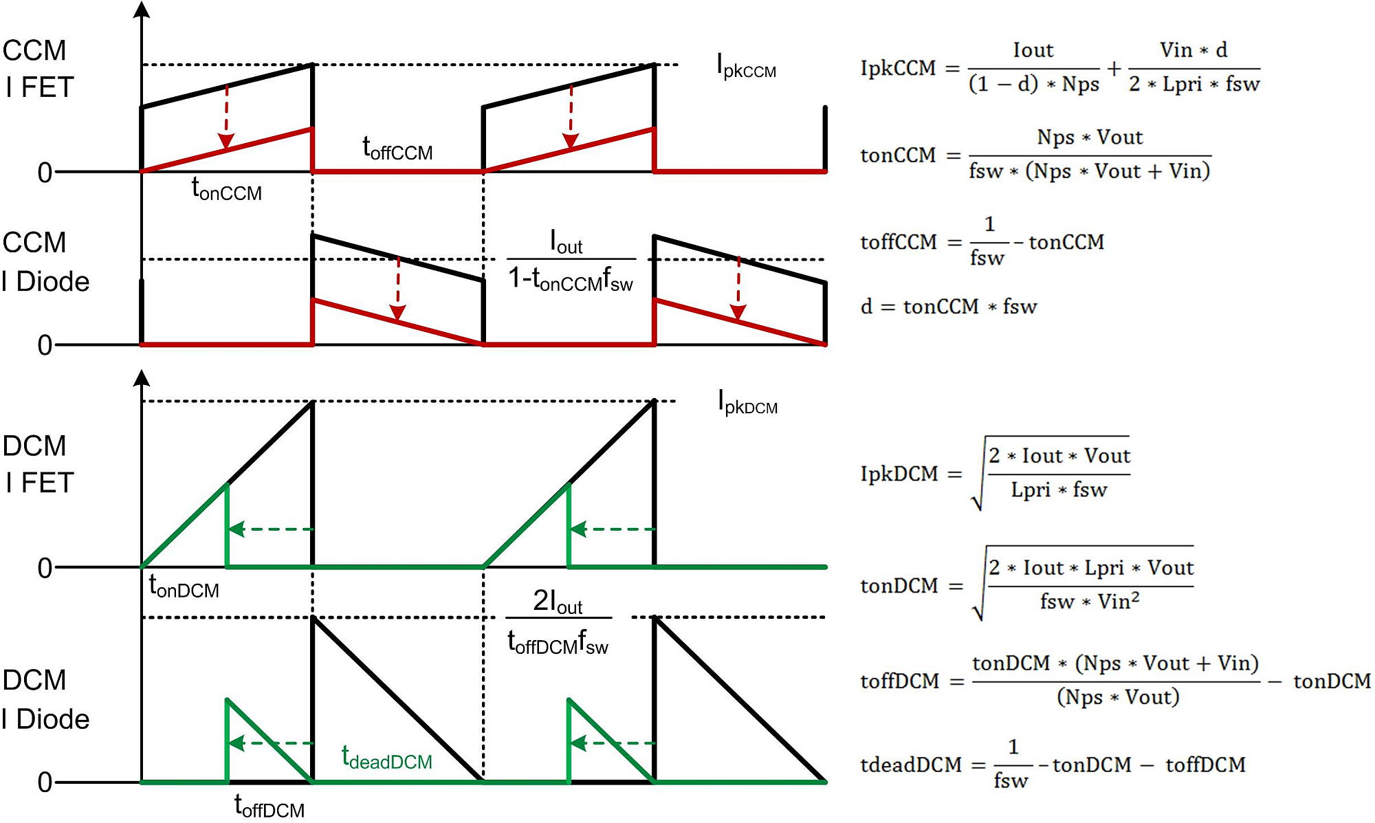
CCM and discontinuous-conduction mode (DCM) operation each have their own merits. By definition, DCM operation occurs when the output rectifier current decreases to 0A before the next cycle starts. DCM operation benefits include a lower primary inductance typically resulting in a smaller power transformer, elimination of the rectifier’s reverse-recovery losses and FET turn on losses, and no right-half-plane-zero. However, these advantages are offset by higher peak currents in the primary and secondary, increased input and output capacitances, increased electromagnetic interference (EMI), and decreased duty-cycle operation at light-load compared to CCM.
 Figure 2 Comparison of CCM and DCM
flyback FET and rectifier currents,
Figure 2 Comparison of CCM and DCM
flyback FET and rectifier currents,Figure 2 illustrates how currents in Q2 and D1 change while at minimum VIN, and the load decreases from the maximum to ~25% in both CCM and DCM. In CCM, the duty cycle is constant for a fixed-input voltage and when the load is between its maximum and minimum design level (~25%). The current “pedestal” levels decrease with reduced loading until DCM is reached, at which point the duty-cycle decreases. In DCM, maximum duty-cycle only occurs at minimum VIN and maximum load. The duty cycle decreases for increased input voltage or reduced load.
This can make the duty-cycle small at high-line and minimum load, so be sure your controller can operate properly at this minimum on-time. DCM operation introduces a dead-time for duty cycles below 50% after the rectifier current reaches 0A. It’s characterized by a sinusoidal voltage on the FET drain and set by residual current, parasitic capacitances, and leakage inductance, but is generally benign. For this design, CCM operation was chosen because higher efficiency can be achieved from reduced switching and transformer losses.
This design uses a primary referenced 14V bias winding to power the controller after the 12V output reaches regulation, reducing losses versus being directly powered from the input. I chose a two-stage output filter for low-ripple voltage. The first-stage ceramic capacitors handle the high RMS current from the pulsating currents in D1. Their ripple voltage is reduced by filter L1 and C9/C10, providing about 10 times the ripple reduction along with reduced RMS currents in C9/C10. If a higher output ripple voltage is acceptable, the inductor-capacitor filter can be eliminated, but the output capacitors must be capable of handling the full RMS current.
The UCC3809-1 or UCC3809-2 controller is designed to interface directly with the U2 optocoupler for an isolated application. In non-isolation designs, U2 and U3 can be eliminated along with the voltage-feedback resistor-divider connected directly to a controller, such as the UCC3813-x series with internal error amplifier.
Switching voltages on Q2 and D1 create high-frequency common-mode currents in the transformer interwinding and component parasitic capacitances. Without the EMI capacitor C12 providing a return path, these currents would flow into the input and/or output, increasing noise or possibly erratic operation.
The combination of Q3/R19/C18/R17 provides slope-compensation by summing the oscillator’s voltage-ramp into the primary current-sense voltage of R18, which is used for current-mode control. Slope-compensation eliminates sub-harmonic oscillation, a phenomena characterized by a wide duty-cycle pulse followed by a narrow one. Since this converter is designed to not exceed 50% operation, instead I added slope compensation to reduce switch-jitter susceptibility. However, excessive voltage-slope can push the control loop towards voltage-mode control and possible instability. Finally, the optocoupler transfers the error-signal from the secondary-side to keep the output voltage regulated. The feedback (FB) signal comprises the current-ramp, slope-compensation, output error signal, and DC offset to reduce the over-current threshold.
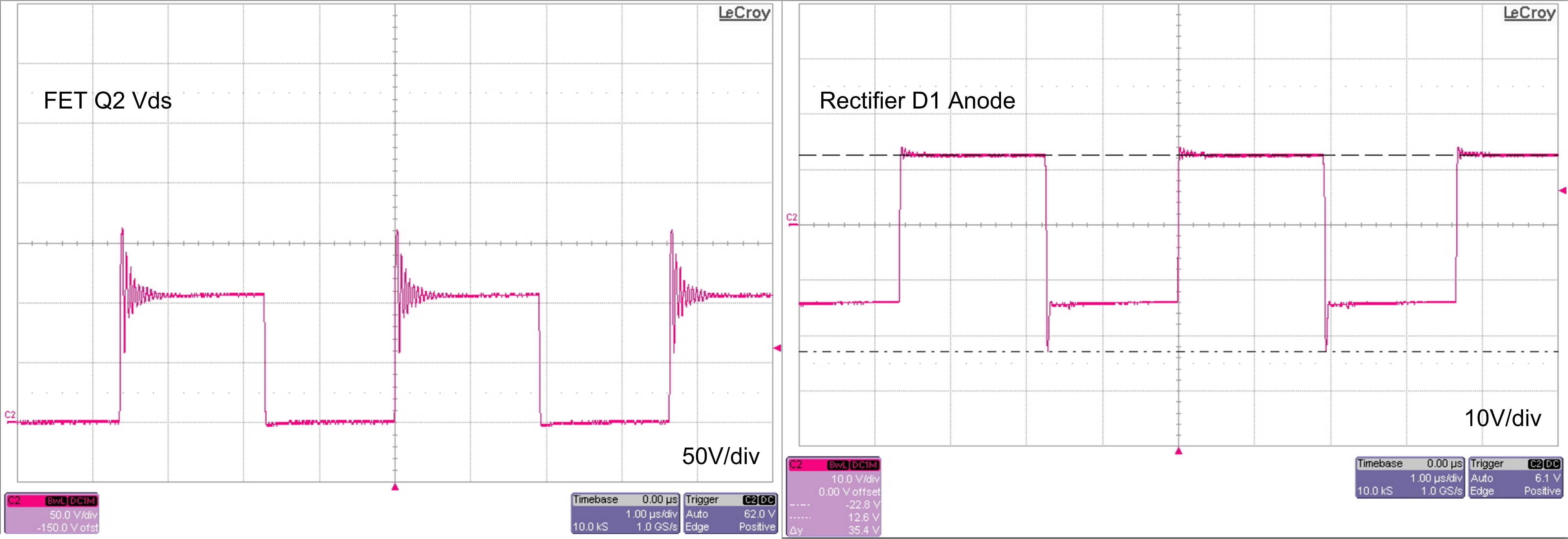
Figure 3 shows the voltage waveforms for Q2 and D1, displaying some leakage inductance and diode reverse-recovery induced ringing.
 Figure 3 FET and rectifier ringing are
limited with a clamp and snubber (57 VIN, 12 V at 5 A).
Figure 3 FET and rectifier ringing are
limited with a clamp and snubber (57 VIN, 12 V at 5 A).Flybacks are considered the standard in applications requiring a low-cost, isolated converter. This design example covers basic design considerations for a CCM flyback design.
Check out TI’s Power Tips blog series on Power House.
Also see :
- Power Tips #75: USB Power Delivery for automotive systems
- How to design a flyback converter as a front-end for a two-stage LED driver
- LTC Design Note: 560V Input, no-opto isolated flyback converter
- Quasiresonant flyback converter easily charges energy-storage capacitors
- Why use a BJT in a flyback converter?
Previously published on EDN.com.