SSZTCV7 February 2024 TMS320F280025C , TMS320F280039C , TMS320F280049C
When designing a digital power supply such as boost power factor correction (PFC), have you ever seen a current oscillate like it does in Figure 1?
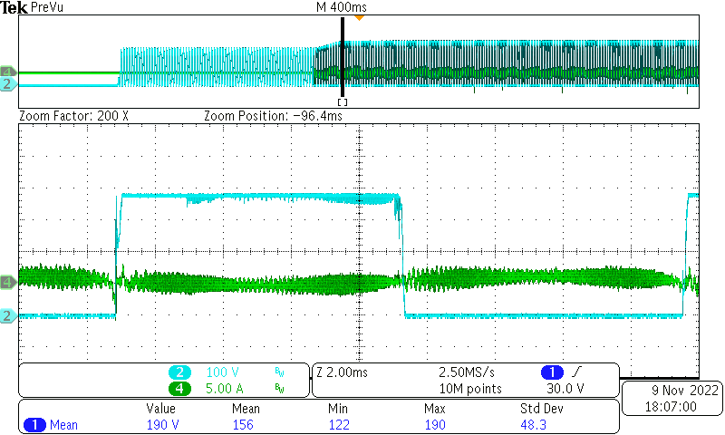 Figure 1 Current oscillation happens in
the PFC stage. Source: Texas Instruments
Figure 1 Current oscillation happens in
the PFC stage. Source: Texas InstrumentsYou may think that this unstable oscillation is caused by a too-fast control band, so you reduce the proportional gain (Kp) and integral gain (Ki) of the proportional-integral (PI) controller and significantly reduce the cross frequency. Then the oscillation disappears.
But is that the best solution? The lower current-loop bandwidth reduces the control speed, but you may find that the total harmonic distortion (THD) test fails. And sometimes the oscillation appears again when your source impedance is a little bit large.
Is there another possible cause of this instability? How can you achieve the best control bandwidth with enough phase margin? Let’s analyze the digital control loop in detail, to see how this potential mistake was introduced. We will also show you how to check whether this instability is happening in your control firmware.
MCU-based digital control
Figure 2 illustrates an MCU-based digital control system.
 Figure 2 The digital control system is
built around a microcontroller. Source: Texas Instruments
Figure 2 The digital control system is
built around a microcontroller. Source: Texas InstrumentsThe control loop includes an analog-to-digital converter (ADC) for sampling the object current/voltage, a digital controller for generating the adjust value, and a pulse-width modulator (PWM) for executing the adjustment, changing the target current/voltage by changing the duty or frequency.
ADC sampling in a switched-mode power supply (SMPS) is often at the middle points of two switching cycles, which not only avoids noise disturbances from switching, but also gets the average current value of the power inductor in continuous conduction mode (CCM).
The digital controller is calculated in an interrupt service routine (ISR) and could be triggered synchronously with the PWM output. The trigger event could be one of these occurrences: the PWM’s "COUNTER" equals "ZERO," "PERIOD," or a specific value "CMP."
It is not possible to update the PWM immediately when the controller completes all calculations, but the PWM registers must be loaded by shadow registers at a dedicated moment, such as when the PWM counter equals "ZERO" or "PERIOD". If the PWM values are changed while the counter is rising or falling, it is very possible to generate false PWM action, missing pulses or duplicating pulses.
Unlike an analog control system, digital control is executed by the sampling frequency, and there must be a delay time (Td ) from sampling to reloading a new value to the PWM. PWM modification is implemented by adjusting the flipping moments, which happens once with single-edge modulation (count up/count down mode), and happens twice with dual-edge modulation (count up-down mode). So, the minimum Td will be one switching cycle Ts , (as shown in Figure 3a) or one-half switching cycle Ts/2, (as shown in Figure 3b), depending on the modulation reloading frequency that you choose.
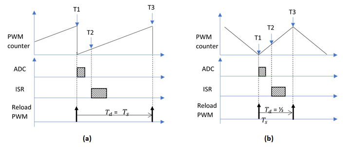 Figure 3 Minimum delay time is
introduced by PWM adjusting: (a) up mode, (b) up-down mode. Source: Texas
Instruments
Figure 3 Minimum delay time is
introduced by PWM adjusting: (a) up mode, (b) up-down mode. Source: Texas
InstrumentsLooking at Figure 4, Td would be expressed as e-sxT d in its transfer function, which would reduce the phase margin. Of course, when the phase margin is less than 45 degrees, the system will become unstable and oscillation will occur.
 Figure 4 The influence of time delay is
shown in the Bode plot. Source: Texas Instruments
Figure 4 The influence of time delay is
shown in the Bode plot. Source: Texas InstrumentsA potential code mistake in digital control implementation
With correct execution, the minimum Td is one switching cycle Ts half switching cycle Ts/2. But if you haven’t considered the consequence of ADC, ISR and PWM reloading, it is possible that extending the control delay to more than one switching cycle may reduce phase margin and lead to instability.
For example, in Figure 5 the ADC’s ISR trigger and PWM reload start at the same moment, when the PWM counter equals zero.
Although all blocks execute at the same time, can you expect Td to be zero in this case? Absolutely not!
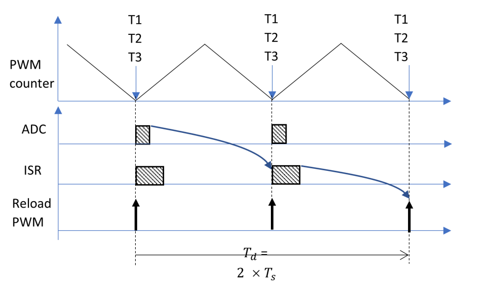 Figure 5 Here is an example of wrong
code introducing a larger delay time. Source: Texas Instruments
Figure 5 Here is an example of wrong
code introducing a larger delay time. Source: Texas InstrumentsThis is because both the ADC conversion and ISR calculation require far more than one MCU clocking cycle - the ADC conversion still hasn’t completed when the ISR reads the ADC result. Thus, the ISR will get the "old" sample value for calculating, and the calculation for the latest value is delayed until the next switching cycle. After the completion of the ISR calculation, the new PWM value is only written into the shadow register, which will be reloaded in the next switching cycle. In reality the total control delay of Td will be two switching cycles, or 2 x Ts .
Besides the examples shown here, other implementations may introduce similar extended control delays - for example, if you put the ADC value reading after the controller calculation in the ISR code, or if you add an N-cycles algorithm average before calculating the controller.
As shown in Figure 6, when you set the GAIN cross frequency at around 3 kHz with the false implementation of Figure 5, the phase margin is 41.68 degrees. This is less than 45 degrees, and the choke current has significant oscillation, like the waveform of Figure 1, so you are forced to reduce the cross frequency to lower than 2 kHz; then the iTHD turns worse and fail the requirements.
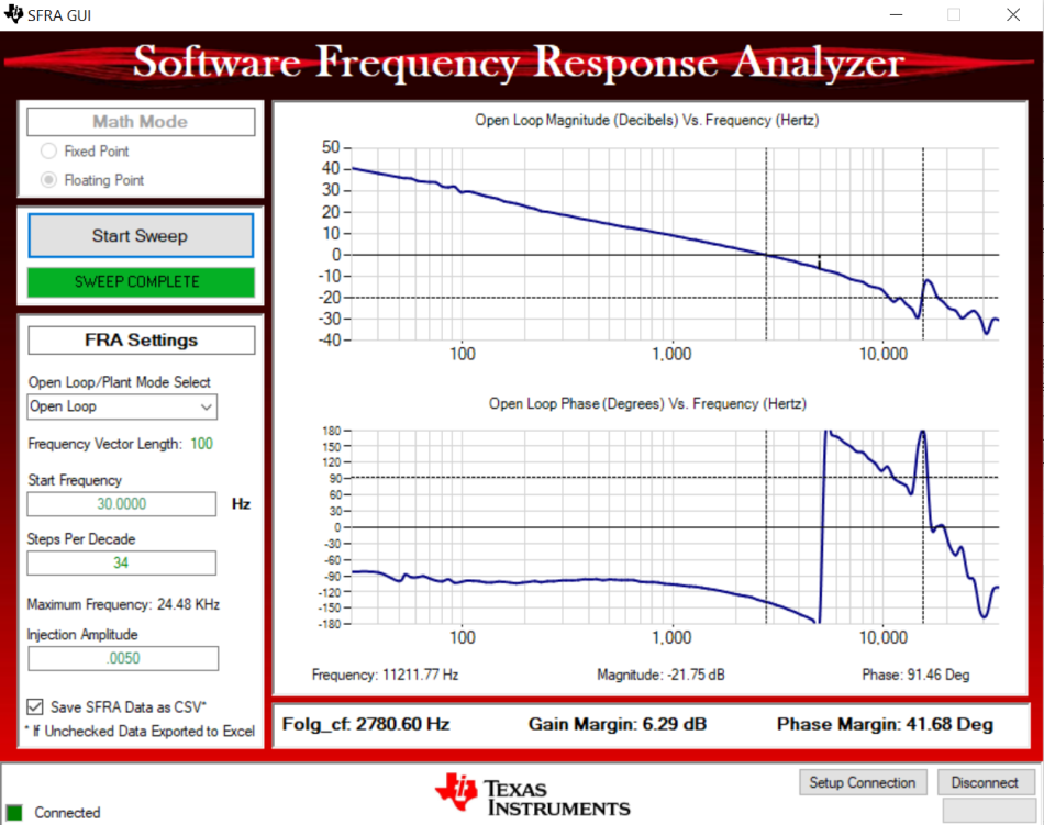 Figure 6 Bode plot with the wrong code
implementation. Source: Texas Instruments
Figure 6 Bode plot with the wrong code
implementation. Source: Texas InstrumentsDesign solution
You can easily fix this problem by moving the ADC conversion to the moment of counter = period and have PWM reloading occur in the next counter = period, as shown in Figure 7.
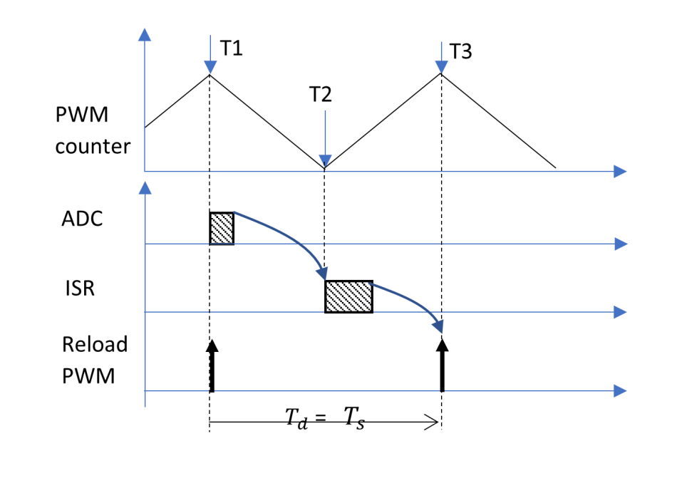 Figure 7 The control delay can be
reduced with code improvement. Source: Texas Instruments
Figure 7 The control delay can be
reduced with code improvement. Source: Texas InstrumentsThe control delay will be reduced to one switching cycle. The phase margin increases significantly, and the current oscillation disappears, as shown in Figure 8 and Figure 9.
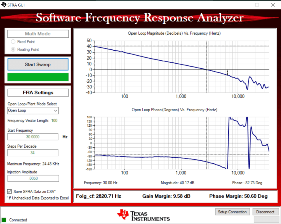 Figure 8 Bode plot with improved code.
Source: Texas Instruments
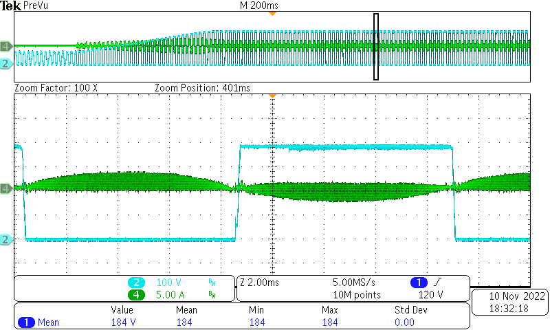 Figure 9 Waveform with improved code.
Source: Texas Instruments
Figure 9 Waveform with improved code.
Source: Texas InstrumentsWell-organized control scheme
The control delay in a digital implementation, from ADC sampling to PWM adjustment, will reduce the phase margin and cause oscillation. When tackling this issue, consider the consequence of ADC sampling, controller calculation and PWM reloading. A well-organized control scheme can minimize the delay to one-half, or one switching cycle, which increases the phase margin and loop bandwidth.
Related Content
- Power Tips #113: Two simple isolated power options for 8 W or less
- Power Tips #112: Onboard fixtures for fault testing
- Power Tips #111: Why current sensing is a must in collaborative, mobile robots
- Power Tips #110: How parasitics create an unexpected EMI filter resonance
- The basics of doing PID design: Part 1 – Classical control theory
- Testing a power supply – Stability (Part 3)
Previously published on EDN.com.