-
Adding a single capacitor to improve cross-regulation in dual-output flyback power supplies
Adding a single capacitor to improve cross-regulation in dual-output flyback power supplies
Brian King
Systems that require multiple output voltages typically employ flyback converters. In these multiple-output flyback converters, maintaining good regulation simultaneously on all output voltages is a big challenge.
Power Tips #78 explored how using synchronous rectifiers can improve cross-regulation between output voltages. The synchronous rectifiers balance the output voltages, but the trade-off is higher root-mean-square (RMS) current in the windings and decreased efficiency at light loads. In this power tip, I’ll continue the discussion by looking at a special case that generates positive/negative outputs of the same magnitude. In this situation, proper placement of a single capacitor can improve cross-regulation across all loading conditions.
Figure 1 shows a simplified schematic of a 48-V to ±12-V supply in its normal configuration. To implement the technique proposed here, you must first shuffle the secondary connections around a little, as shown in Figure 1 , by adding capacitor C3 and moving diode D2 from the low side of the secondary winding to the high side. Also, notice that the two transformer secondary windings no longer share a common connection. Other than the added capacitor, C3, Figure 1 is electrically equivalent to Figure 1 .
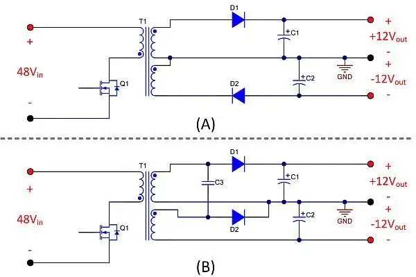 Figure 1 Typical configuration of
dual-output flyback supplies (a); reconfiguring and adding a capacitor as shown
improves cross-regulation (b).
Figure 1 Typical configuration of
dual-output flyback supplies (a); reconfiguring and adding a capacitor as shown
improves cross-regulation (b).Figure 2A shows the state of the circuit when Q1 is off and both D1 and D2 are conducting. During this state, the transformer delivers energy to both outputs through the secondary windings. Notice that C3 is connected in parallel with the +12-V output, and thus charges to the same voltage level.
Figure 2B shows the state of the circuit when Q1 is on and both D1 and D2 are reverse-biased and in the off state. During this state, energy is being stored magnetically in the transformer as the primary winding charges from the input voltage. In this state, as long as both secondary windings have the same number of turns, the voltage across C3 is equal to the magnitude of the −12-V output, as described by the equation shown in Figure 2B. As the circuit alternates between these two states, capacitor C3 acts as a charge pump, helping keep the magnitude of both output voltages balanced. This charge-pump effect compensates for voltage imbalances caused by parasitic elements in the circuit. If the two secondary windings have a different number of turns, this technique will not work.
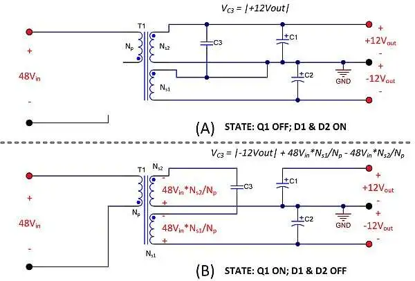 Figure 2 Two states of the circuit: Q1
off, D1 and D2 on (a); Q1 on, D1 and D2 off (b).
Figure 2 Two states of the circuit: Q1
off, D1 and D2 on (a); Q1 on, D1 and D2 off (b).Figure 3 shows a simulation schematic modeling the leakage inductances on the primary and secondary windings. As detailed in Power Tips #78, these leakage inductances cause large differences in regulation. The leakage inductance on the primary causes a short duration voltage pedestal to appear on the primary, which couples across to the secondary windings. The leakage inductances on the secondary windings degrade the coupling between the two output voltages.
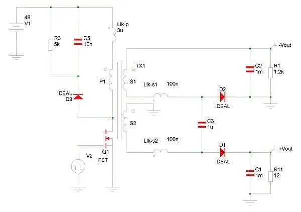 Figure 3 Schematic of a simulation
model to investigate the effects of leakage inductance on output-voltage
regulation.
Figure 3 Schematic of a simulation
model to investigate the effects of leakage inductance on output-voltage
regulation.Figure 4 shows the voltage and current waveforms in the output diodes when loading the +12-V output with 1 A and the −12-V output with 10 mA. Adding the 1-µF capacitor C3 not only keeps the two outputs well-coupled, but also filters the effects of the voltage pedestal caused by the leakage on the primary winding. Notice the small oscillation on the diode voltage of the more lightly loaded −12-V output. This oscillation is caused by leakage inductances resonating with capacitor C3, and results in a phase shift in the conduction of the −12-V output diode. The current waveform shapes are interesting in that the −12-V current maintains a triangular shape, which subtracts from the +12-V secondary winding current.
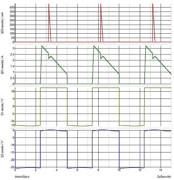 Figure 4 Voltage and current waveforms
on the output diodes, with the +12-V output loaded at 1 A and the -12 V loaded
at 10 mA.
Figure 4 Voltage and current waveforms
on the output diodes, with the +12-V output loaded at 1 A and the -12 V loaded
at 10 mA.The graph of Figure 5 shows the regulation impacts of adding the capacitor. Here, simulations are plotted with different loading conditions on the two outputs, both with and without the added capacitor.
Without the capacitor, the −12-V output voltage rises significantly, as the −12-V load decreases toward zero. With the capacitor, both outputs track each other within 3% across the entire load range. These results are similar to those obtained by using synchronous rectifiers, as detailed in Power Tips #78, but without the penalty of increased RMS winding currents, and with very little added cost or complexity.
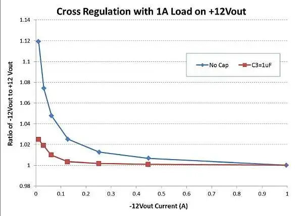 Figure 5 Simulation results show how adding a single capacitor greatly improves cross-regulation.
In conclusion, parasitic leakage inductances conspire to degrade regulation in multiple output power supplies. In supplies with dual positive and negative outputs of equal magnitude, adding a single capacitor can vastly improve the regulation.
In multiple output supplies with different output voltage magnitudes, using synchronous rectifiers is probably the best approach for improving cross-regulation.
The next time you are designing a dual-output power supply, consider implementing this simple technique to improve the performance of your design.
For more Power Tips, check out TI’s Power Tips blog series on Power House.
Additional Resources
- Watch the video, “Topology Tutorial: What is a Flyback?”
- Download TI’s fly-buck and flyback selector tool to help select the right isolated DC/DC topology based for your specification.
IMPORTANT NOTICE AND DISCLAIMER
TI PROVIDES TECHNICAL AND RELIABILITY DATA (INCLUDING DATASHEETS), DESIGN RESOURCES (INCLUDING REFERENCE DESIGNS), APPLICATION OR OTHER DESIGN ADVICE, WEB TOOLS, SAFETY INFORMATION, AND OTHER RESOURCES “AS IS” AND WITH ALL FAULTS, AND DISCLAIMS ALL WARRANTIES, EXPRESS AND IMPLIED, INCLUDING WITHOUT LIMITATION ANY IMPLIED WARRANTIES OF MERCHANTABILITY, FITNESS FOR A PARTICULAR PURPOSE OR NON-INFRINGEMENT OF THIRD PARTY INTELLECTUAL PROPERTY RIGHTS.
These resources are intended for skilled developers designing with TI products. You are solely responsible for (1) selecting the appropriate TI products for your application, (2) designing, validating and testing your application, and (3) ensuring your application meets applicable standards, and any other safety, security, or other requirements. These resources are subject to change without notice. TI grants you permission to use these resources only for development of an application that uses the TI products described in the resource. Other reproduction and display of these resources is prohibited. No license is granted to any other TI intellectual property right or to any third party intellectual property right. TI disclaims responsibility for, and you will fully indemnify TI and its representatives against, any claims, damages, costs, losses, and liabilities arising out of your use of these resources.
TI’s products are provided subject to TI’s Terms of Sale (www.ti.com/legal/termsofsale.html) or other applicable terms available either on ti.com or provided in conjunction with such TI products. TI’s provision of these resources does not expand or otherwise alter TI’s applicable warranties or warranty disclaimers for TI products.
Mailing Address: Texas Instruments, Post Office Box 655303, Dallas, Texas 75265
Copyright © 2024, Texas Instruments Incorporated