-
High-frequency resonant converter design considerations, Part 2
High-frequency resonant converter design considerations, Part 2
Sheng-Yang Yu
The first installment of this series focused on the key parasitic parameters affecting resonant converter design, along with component selection criteria and transformer design. This installment focuses on resonant converter synchronous rectifier (SR) design considerations.
The operational states in a resonant converter can be much more complex than in a pulse-width modulation converter. Taking the inductor-inductor-capacitor-series resonant converter (LLC-SRC) in Figure 1 as an example, there are four common states (Figure 2) in a regular LLC-SRC design with given load conditions and relative positions of switching frequency (fsw) and series resonant frequency (fr). When fsw r, the rectifier diode current goes to zero before an active switch (Q1 or Q2) turns off. Therefore, when applying a metal-oxide semiconductor field-effect transistor (MOSFET) as a rectifier (that is, an SR), the SR must be turned off with less than a 50% duty cycle to avoid rectifier current backflow. Otherwise, the converter efficiency will be harmed by excessive circulating current.
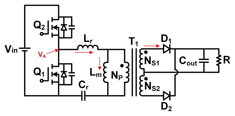 Figure 1 An inductor-capacitor series
resonant converter (LLC-SRC) provides soft-switching features that allow
high-frequency operation.
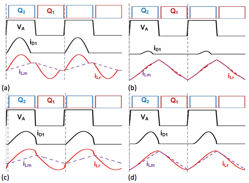 Figure 2 Operational states of an
LLC-SRC under heavy load and fswr (a), light load and fsw
r (b), heavy load and fsw >fr (c), and light load and
fsw >fr (d) show the need of current sensing to
avoid reverse current flow on the output rectifier if SR is applied.
Figure 2 Operational states of an
LLC-SRC under heavy load and fswr (a), light load and fsw
r (b), heavy load and fsw >fr (c), and light load and
fsw >fr (d) show the need of current sensing to
avoid reverse current flow on the output rectifier if SR is applied.The rectifier current conduction time is actually 0.5/fr at a heavy load when fsw r . So it is possible to limit the SR conduction time to be slightly less than 0.5/fr at a heavy load when fsw r and disable the SR at a lighter load [1]. This open-loop SR control method won’t be able to optimize converter efficiency, however.
A more reliable SR control method is through MOSFET drain-to-source voltage (VDS) sensing [2] (Figure 3). Basically, this SR control method compares the MOSFET VDS with two different voltage thresholds to turn the MOSFET on and off. Some newer VDS sensing SR controllers like the UCC24624 from Texas Instruments even have a third voltage threshold to activate a proportional gate driver for fast SR turn off with minimal delay.
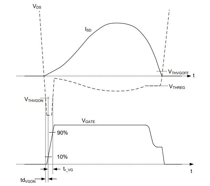 Figure 3 VDS sensing SR
turns SR on and off at different VDS voltage levels.
Figure 3 VDS sensing SR
turns SR on and off at different VDS voltage levels.It is notable that the voltage thresholds are in the millivolt levels; high-accurate sensing circuitry is required. Therefore, the VDS sensing method is generally realized by using integrated circuits, which have a VDS level (less than 200V in general) and fsw limitations (less than 400kHz in general). Due to the limitations the VDS sensing SR control method have, you will need a different SR control method to optimize SR conduction for high-voltage and high-frequency resonant converters.
Using a Rogowski coil [3] followed by integrator and comparators is an alternative way to control a high-frequency resonant converter SR. Figure 4 is a block diagram illustrating SR control with a Rogowski coil on a capacitor-inductor-inductor-inductor-capacitor series resonant dual active bridge converter (CLLLC-SRes-DAB) [4]. An air core coil with windings – a Rogowski coil – is placed on the transformer winding for current sensing. When a time-varying current flows through the coil, the current-generated magnetic flux induces voltage on the coil windings. The induced voltage will have a 90-degree phase difference when compared to the original time-varying current.
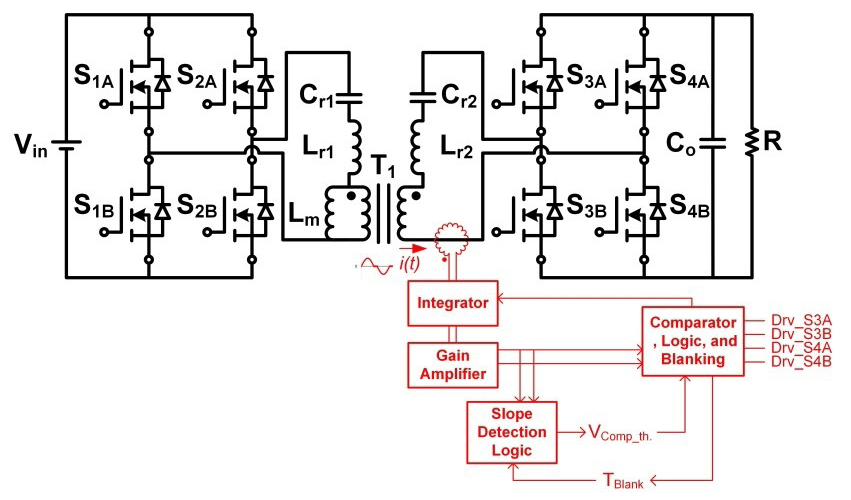 Figure 4 Rogowski coil SR control
enables accurate high-frequency SR sensing and control in a CLLLC-SRes-DAB
converter.
Figure 4 Rogowski coil SR control
enables accurate high-frequency SR sensing and control in a CLLLC-SRes-DAB
converter.Adding an integrator after the Rogowski coil can generate a voltage that is in phase or even leading the original time-varying current. Thus, it is possible to set the zero voltage crossing of the integrator output to be a little bit earlier than the time-varying current zero current crossing to accommodate possible propagation and control delay. The amplified integrator output signal is then compared with a given comparator threshold to generate a SR driving signal with a nearly optimized SR conduction time. Additional slope detection logic inserted in the control circuit further optimizes SR conduction times over different load conditions. Because a Rogowski coil senses current by magnetic flux, there is no voltage-level limitation. Also, a Rogowski coil uses air core instead of magnetic core material, so its bandwidth is very high without saturation limit; thus, there are no frequency limitation concerns even on megahertz level resonant converters unlike the VDS sensing SR control method.
Figure 5 illustrates the method proposed here. Defining the time-varying current in Figure 5 to be i(t) and assuming that the Rogowski coil is placed vertically on the transformer winding, you can use Equation 1 to calculate the Rogowski coil winding output voltage as:
where A is the cross-section area of each turn on the Rogowski coil (assuming that the turns on the Rogowski coil all have the same area of the cross section), N is the number of turns on the Rogowski coil, l is the circumference of the Rogowski coil ring, and μ0 = 4π ∙ 10-7 H/m is the permeability constant.
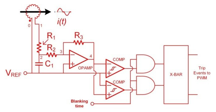 Figure 5 Passive integrator allows the
Rogowski coil SR control circuit to predict the zero current crossing
timing.
Figure 5 Passive integrator allows the
Rogowski coil SR control circuit to predict the zero current crossing
timing.Assuming the use of an ideal operational amplifier used in the proposed sensing circuit, Equation 2 expresses the voltage relationship between the Rogowski coil output v1_0 and the passive integrator output v2_0:
It’s possible to solve the differential equation in Equation 2 in the form of Equation 3
where a 0 is a constant, expressed by Equation 4.
To more easily understand how to adjust the phase difference with the passive integrator and amplifier, assume that the time-varying current is purely sinusoidal, which will make both the Rogowski coil output voltage and the integrator output purely sinusoidal. In other words, solving Equation 1 and Equation 2 to get the solution of i(t) with the assumption of v 2_0 (t ) = a 1 sin (ωt ), Equation 2 can be rewritten as Equation 5:
where Equation 6
Flipping the pinouts of the Rogowski coil, the time-varying current becomes Equation 7:
When making Φ = −π/2 for Equation 3 and Φ = π/2 for Equation 4 by varying the values of R1 , R2 , C1 and the fsw (ω = 2πfsw ) with the right connection polarity between the Rogowski coil output and integrator input, the integrator output v 2_0 (t ) can be in phase with the SR current i(t). Moreover, in practical applications, you can set the integrator waveform to lead the SR current. So with the response time and propagation delay on the controller and driver, respectively, the SR turn off timing can still manage to be at the zero current crossing point.
Figure 6 shows the winding current measurement and gain amplifier output voltage of the sensing circuit. As you can see, programming zero voltage crossing to turn off earlier than the actual sensing current accommodates propagation and control delays.
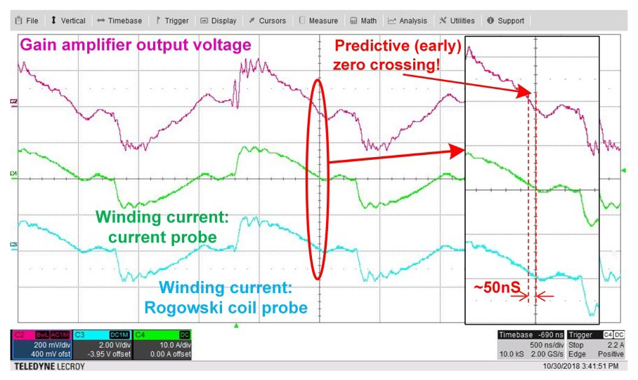 Figure 6 This SR current measurement
comparison shows the predictive SR sensing by having zero current crossing at
integrator output earlier than actual zero current crossing.
Figure 6 This SR current measurement
comparison shows the predictive SR sensing by having zero current crossing at
integrator output earlier than actual zero current crossing.Figure 7 shows perfect SR turn-off timing when the switching frequencies are below the series resonant frequency.
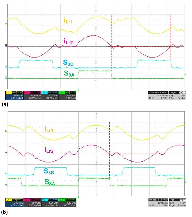 Figure 7 SRs are turning off at perfect
zero current crossing at 300 kHz (a) and 400 kHz (b).
Figure 7 SRs are turning off at perfect
zero current crossing at 300 kHz (a) and 400 kHz (b).References
- J. Wang and B. Lu, “Open loop synchronous rectifier driver for LLC resonant converter,” in Proc. APEC, 2013, pp. 2048-2051.
- UCC24624 dual-channel synchronous rectifier controller for LLC resonant converters, Texas Instruments
- M.H. Samimi, A. Mahari, M.A. Farahnakian and H. Mohseni, “The Rogowski Coil Principles and Applications: A Review,” IEEE Sensors Journal, vol. 15, pp. 651-658, 2015.
- B. Zhao, Q. Song, W. Liu and Y. Sun, “Overview of Dual-Active-Bridge Isolated Bidirectional DC-DC Converter for High-Frequency-Link Power-Conversion System,” IEEE Transactions on Power Electronics, vol. 29, pp. 4091-4106, 2014.
Related articles
- Power Tips #89: High-frequency resonant converter design considerations, Part 1
- Using quasi-resonant and resonant converters
- Measure small impedances with Rogowski current probes
- High efficiency resonant mode implementation using digital control
- Power Tips #84: Think outside the LLC series resonant converter box
Previously published on EDN.com.