SSZTCW6 February 2024 UCC28C50
Flyback converters can operate either in continuous-conduction mode (CCM) or discontinuous-conduction mode (DCM). For many low-power and low-current applications, though, the DCM flyback converter can provide a more compact and lower-cost option. Here is a step-by-step methodology to guide you through such a design.
DCM operation is characterized by the converter having its rectifier current decreasing to zero before the start of the next switching cycle. Decreasing the current to zero before switching will reduce dissipation in the field-effect transistor (FET) and reduce rectifier losses, and will often reduce the transformer size requirement as well.
By comparison, CCM operation maintains rectifier current conduction through the end of the switching period. We covered flyback design trade-offs and power-stage equations for a CCM flyback in Power Tips #76: Flyback converter design considerations and Power Tips #77: Designing a CCM flyback converter. CCM operation is best suited for medium- to high-power applications, but if you have a low-power application that could use a DCM flyback, read on.
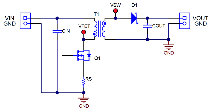
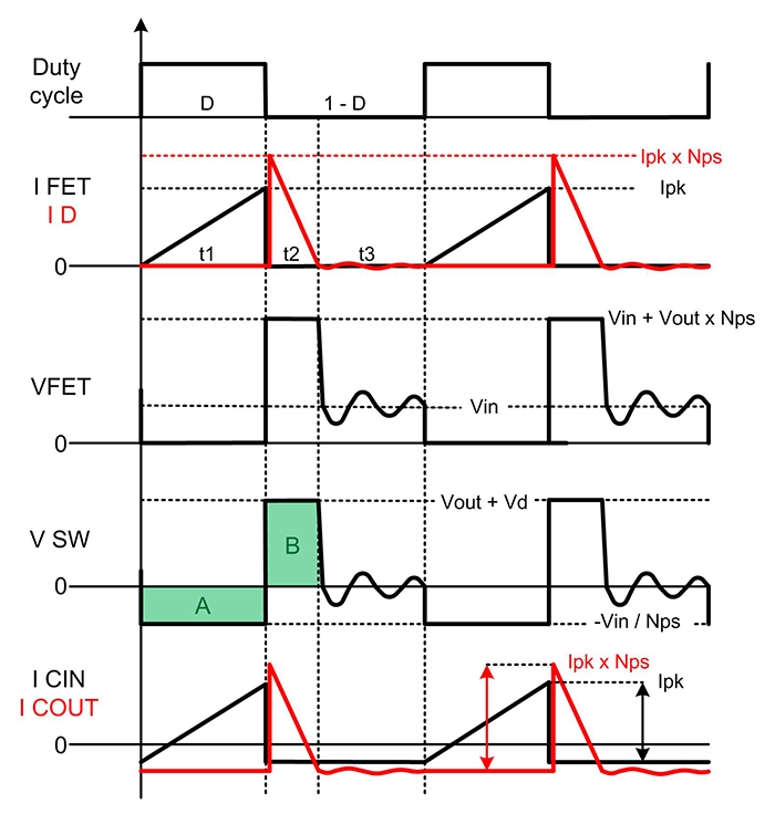
Figure 1 shows a simplified flyback schematic, which can operate in either DCM or CCM mode. Further, the circuit can switch between modes depending on timing. To maintain operation in DCM mode, which is what this article will evaluate, the key component switching waveforms should have the characteristics shown in Figure 2.
Operation starts when FET Q1 turns on for duty cycle period D. The current in T1’s primary winding, which always starts at zero, reaches a peak set by the primary winding inductance, the input voltage, and on-time t1. During this FET on-time, diode D1 is reverse-biased because of T1’s secondary winding polarity, forcing all output current to be supplied by output capacitor COUT during time periods t1 and t3.
 Figure 1 This simplified flyback
converter can operate in either DCM or CCM.
Figure 1 This simplified flyback
converter can operate in either DCM or CCM.When Q1 turns off during period 1-D, T1’s secondary voltage polarity reverses, which allows D1 to conduct current to the load and recharge COUT. Current in D1 decreases linearly from its peak to zero during time t2. Once T1’s stored energy is depleted, only residual ringing occurs during the remainder of period t3. This ringing is primarily due to T1’s magnetizing inductance and to the parasitic capacitances of Q1, D1, and T1. This is easily seen in Q1’s drain voltage during t3, which drops from VIN plus the reflected output voltage back to VIN, since T1 cannot support a voltage once current flow stops. (Note: Without an adequate dead time for t3, CCM operation may occur.) Currents in CIN and COUT are identical to those in Q1 and D1, but without a DC offset.
Shaded areas A and B in Figure 2 highlight the transformer’s volt-microsecond products during t1 and t2, which must be in balance to prevent saturation. Area “A” represents (Vin/Nps) × t1 while “B” represents (Vout + Vd) × t2, both referenced to the secondary side. Np/Ns is the transformer primary-to-secondary turns ratio.
 Figure 2 The key voltage and current
switching waveforms for a DCM flyback include several critical parameters that
designers must specify.
Figure 2 The key voltage and current
switching waveforms for a DCM flyback include several critical parameters that
designers must specify.Table 1 details characteristics of DCM operation relative to CCM. One key DCM attribute is that having a lower primary inductance decreases the duty cycle, regardless of the transformer’s turns ratio. This attribute lets you constrain your design’s maximum duty cycle. This can be important if you are trying to use a specific controller or stay within certain on or off time limits. A lower inductance, which requires a lower average energy storage (albeit with a higher peak FET current), also often results in allowing a smaller transformer than a CCM design would require.
Another DCM advantage is that the design eliminates D1 reverse-recovery losses in standard rectifiers, since the current is zero at the end of t2. Reverse-recovery losses often appear as increased dissipation in Q1, so eliminating them reduces stresses on the switching transistor. The benefit of this becomes increasingly important at higher output voltages, where the reverse-recovery times of rectifiers increase with higher-voltage-rated diodes.
| DCM advantages | DCM disadvantages |
|---|---|
| Lower primary inductance than CCM | Higher peak primary current |
| Inductance sets the maximum duty cycle | Higher peak rectifier current |
| Smaller transformer possible | Increased input capacitance |
| No rectifier reverse-recovery losses | Increased output capacitance |
| No (or minimal) FET turn-on losses | Potentially increased electromagnetic interference |
| No right half-plane zero in the control loop | Wider duty-cycle operation than CCM |
| Optimal for low output power | Increased bandwidth variation |
Developers will need to know several key parameters when starting a design, along with the basic electrical specification. Begin by selecting a switching frequency (fsw), a maximum desired operating duty cycle (Dmax), and an estimated target efficiency. Equation 1 then calculates on time t1 as:
Next, estimate the transformer’s peak primary current, Ipk, using Equation 2. For the FET’s on voltage (Vds_on) and the current-sense resistor voltage (VRS) in Equation 2, assume small voltage drops that are appropriate for your design, like 0.5 V. You can update these voltage drops later.
Equation 3 calculates the required transformer turns ratio, Np/Ns, based on equating areas A and B in Figure 2:
where x is a desired minimum idle time for t3 (starting with x = 0.2).
If you would like to change Np/Ns, adjust Dmax and iterate again.
Next, calculate the maximum “flat-top” voltages for Q1 (Vds_max) and D1 (VPIV_max) using Equation 4 and Equation 5:
Since these components generally have ringing due to transformer leakage inductance, a rule of thumb is to expect the actual values to be 10-30% higher than Equation 4 and Equation 5 predict. If Vds_max is higher than anticipated, reducing Dmax will lower it, but VPIV_max will increase. Determine which component voltage is the more critical and iterate again if necessary.
Calculate t1_max using Equation 6, which should be close to that in Equation 1:
Calculate the maximum required primary inductance with Equation 7:
If you select a lower inductance than Equation 7 indicates, increase x and decrease Dmax until Np/Ns and Lpri_max are equal to your desired values by iterating as necessary.
You can now calculate Dmax in Equation 7:
And calculate the maximum Ipk and its maximum root-mean-square (RMS) value using Equation 9 and Equation 10, respectively:
Calculate the maximum current-sense resistor value allowed, based on the selected controller’s current-sense input minimum current limit threshold, Vcs (Equation 11):
Use the values calculated for Ipkmax in Equation 11 and RS to verify that the assumed voltage drops for the FET Vds and sense resistor VRS in Equation 2 are close; iterate again if significantly different.
Use Equation 12 and Equation 13 to calculate the maximum power dissipated in RS and conduction losses in Q1 from Equation 10:
FET switching losses are generally highest at Vinmax, so it’s best to calculate Q1 switching losses over the full range of VIN using Equation 14:
where Qdrv is the FET total gate charge and Idrv is the expected peak gate-drive current.
Equation 15 and Equation 16 calculate the total power loss from charging and discharging the FET’s nonlinear Coss capacitance. The integrand in Equation 15 should closely match the actual FET’s Coss data-sheet curve between 0 V and its actual operating Vds. Coss losses are generally greatest in high-voltage applications or when using very low RDS(on) FETs, which have larger Coss values.
Total FET losses can be approximated by summing the results of Equation 13, Equation 14, and Equation 16.
Equation 17 reveals that the diode losses in this design will greatly simplify. Be sure to select a diode rated for the secondary peak current, which is generally much greater than IOUT.
Output capacitance is generally selected as the larger of Equation 18 or Equation 19, which calculate capacitance based on ripple voltage and equivalent series resistance (Equation 18) or load transient response (Equation 19):
where ∆IOUT is a change in output load current, ∆VOUT is the allowable output-voltage excursion and fBW is the estimated converter bandwidth.
Equation 20 calculates the output capacitor RMS current as:
Equation 21 and Equation 22 estimate the input capacitor’s parameters as:
Equation 23, Equation 24, and Equation 25 summarize the three key waveform time intervals and their relationship:
If you need additional secondary windings, Equation 26 easily calculates additional winding, Ns2:
where VOUT1 and Ns1 are the regulated output voltage.
The transformer primary RMS current is the same as the FET RMS current in Equation 10; the transformer secondary RMS current is shown in Equation 27. The transformer core must be capable of handling Ipk without saturating. You should consider core losses too, but that is beyond the scope of this article.
As can be seen in the steps provided, the design of a DCM flyback is an iterative process. Some of your initial assumptions, such as switching frequency, inductance, or turn ratios, may change based on later calculations, like power dissipations. But remain diligent and go through the design steps as often as required to achieve the design parameters you need. An optimized DCM flyback design can provide a low-power, compact, and low-cost solution to power converter needs if you are willing to put in the effort.
Related articles
- Power Tips #76: Flyback converter design considerations
- Power Tips #77: Designing a CCM flyback converter
- Power Tips #87: How to design a high-voltage DCM inverting charge pump converter
- How to design a flyback converter as a front-end for a two-stage LED driver
- Implementing power factor correction with frequency clamp critical conduction mode
- Discontinuous conduction brings issues to current-mode converters
Previously published on EDN.com.