SSZTCW8 June 2019 LM5155 , LM51551 , LM5156
Boost converters provide a higher output voltage from a lower input voltage. Getting the most “boost” possible requires maximizing the operational duty cycle.
Boost controllers have a limit on their maximum continuous duty cycle, which is typically highest at lower switching frequencies. If you exceed this maximum duty cycle, pulse skipping occurs, which is generally detrimental and should be avoided. Many controllers have maximum duty cycles in the 80% to 90% range, which may increase by a few percent if they’re operated at a very low switching frequency. Low switching frequencies require larger components and increased circuit board area. But even when operating at low switching frequencies, you still might not be able to get enough boost. So what can you do?
Figure 1 shows a simplified schematic of a traditional boost converter power stage. Its main benefit is its low component count, standard inductor and ability to implement a simple low-side boost controller. A key limitation of this basic boost, however, is that it can only provide a maximum boost ratio of 10-to-1, assuming a 90% maximum duty cycle. If you need more boost, you could try using a flyback or boost converter with a charge-pump doubler. Charge pumps added to a boost are good for low output currents, but require additional components to implement. Flybacks are a reasonable solution as well. But an even simpler solution exists with fewer transformer pins, lower turns ratios and lower leakage inductance.
 Figure 1 A traditional single inductor
boost converter power stage.
Figure 1 A traditional single inductor
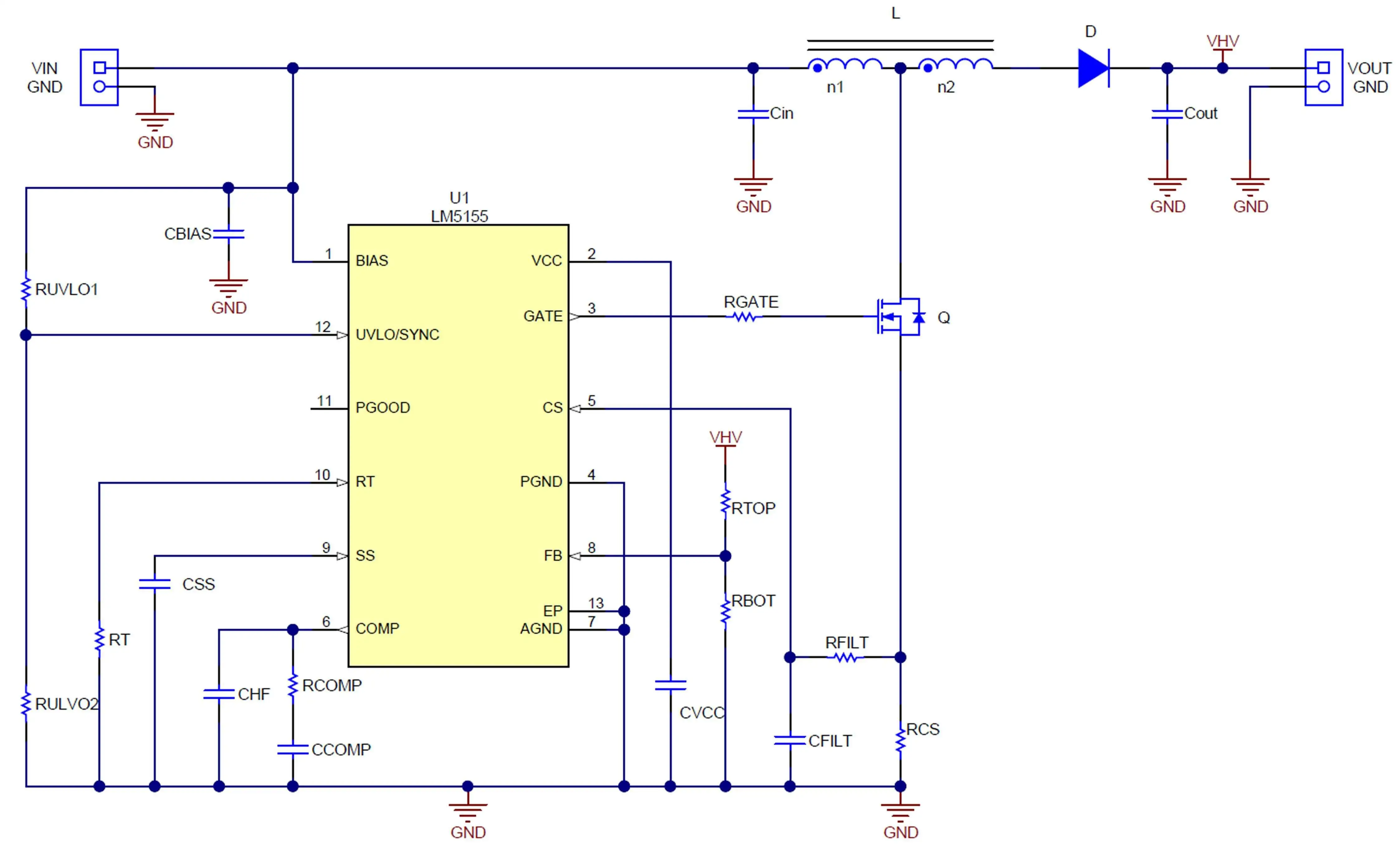
boost converter power stage.Figure 2 shows an autotransformer boost converter. It uses two series-connected windings on the same core, which behaves as a transformer without isolation. Placing the primary in series with the secondary reduces the required turns ratio compared to a flyback, while also requiring fewer pins.
 Figure 2 An autotransformer boost
converter provides a higher output voltage than a traditional boost.
Figure 2 An autotransformer boost
converter provides a higher output voltage than a traditional boost.Equation 1 expresses the duty cycle for operation in continuous conduction mode (CCM) for a given Vin, Vout and n2/n1 turns ratio (ignoring the field-effect transistor [FET] and current-sense resistor drops):
You can see that for a large n2/n1 turns ratio, the duty cycle decreases. This is beneficial for providing a higher output voltage. Equation 2 solves the expression for Vout:
You can see that if n2/n1 = 0, the expression is the same as it is for a traditional boost converter. So for a non-zero n2/n1 turns ratio, Vout increases by an additional amount equal to (n2/n1)*Vin*d/(1-d), so much higher output voltages are possible.
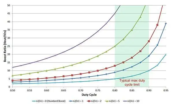
Figure 3 plots the boost ratio, Vout/Vin, versus the duty cycle for several n2/n1 turns ratios, including zero for a traditional boost for comparison. At a 90% duty cycle, the traditional boost has a ratio of 10 compared to 19 for n2/n1 = 1, allowing nearly two times the output voltage. You can easily implement a 1-to-1 n2/n1 ratio with a standard coupled inductor, many of which are readily available. Larger turns ratios can provide a substantially higher output voltage.
 Figure 3 Tapped inductors reduce duty
cycles and enable higher output voltages.
Figure 3 Tapped inductors reduce duty
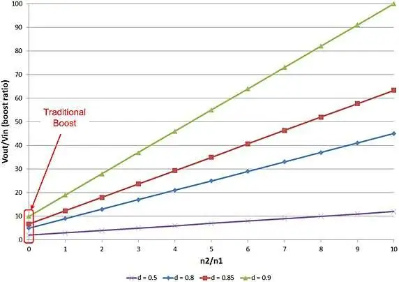
cycles and enable higher output voltages.You will usually know the boost ratio based on design specifications. The maximum practical duty cycle is determined by the controller chosen and the desired switching frequency. Figure 4 shows you how to easily determine the required turns ratio. For example, suppose you need 250 V out from a 10-V input, and wish to limit the maximum duty cycle to 80%. Select the boost ratio of 250 V/10 V = 25 and follow it to the blue curve (d = 0.8); the required n2/n1 is 5.
Equation 3 shows voltage stress for the FET when off, while Equation 4 shows the rectifier reverse voltage stress:
For the design example above, the FET and rectifier voltage stresses are 50 V and 300 V, respectively. The FET voltage stress is considerably lower than a traditional boost, which would have about 250 V across it. Since leakage inductance will be present, an resistor-capacitor snubber may be necessary to reduce ringing.
 Figure 4 Determine your required turns
ratio by selecting your boost ratio and maximum duty cycle.
Figure 4 Determine your required turns
ratio by selecting your boost ratio and maximum duty cycle.Implementing an autotransformer in a CCM boost converter provides several advantages. It increases the output voltage possible beyond that of a traditional boost converter with only the addition of a winding. It reduces the operational duty cycle, enabling higher switching frequencies, smaller component sizes and a lower FET voltage. A reduced duty cycle may also offer a broader selection of controllers that previously could not operate at sufficiently high duty cycles when implemented in a traditional boost converter.
For more Power Tips, check out TI’s Power Tips blog series on Power House.
Related articles
- Protect your boost converter
- Tiny microcontroller hosts dual dc/dc-boost converters
- Use a microcontroller to design a boost converter
- Power Tips #77: Designing a CCM flyback converter
- Power Tips #87: How to design a high-voltage DCM inverting charge pump converter
Previously published on EDN.com.