SSZTCY0 February 2024 UCC28C50
A continuous-conduction mode (CCM) flyback converter is often used in medium power, isolated applications. CCM operation is characterized by lower peak switching currents, less input and output capacitance, reduced EMI, and a narrower operational duty-cycle range than discontinuous-conduction-mode (DCM) operation. These virtues, along with being low cost, mean they have been widely adopted in commercial and industrial applications. This article will provide the power-stage design equations for a 53Vdc to 12V at 5A CCM flyback previously discussed in Power Tips: Flyback converter design considerations.
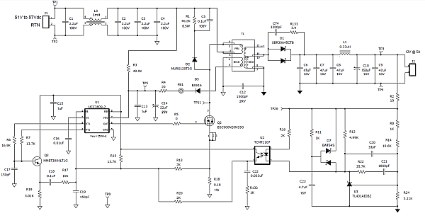
Figure 1 shows a detailed 60W flyback schematic, operating at 250 kHz. The duty-cycle is selected to be 50% maximum at the minimum input voltage of 51V and maximum load. Although operation beyond 50% is acceptable, it is not necessary in this design. The duty cycle will decrease only a few percent while in CCM operation because of the relatively low high-line input voltage of 57V. However, if the load is greatly reduced and the converter enters DCM operation, duty cycle will significantly decrease.
 Figure 1 60W CCM flyback converter
schematic.
Figure 1 60W CCM flyback converter
schematic.Design specifics
To prevent core saturation, the volt-second product for the windings on/off times must balance. This equates to Equation 1:
Set dmax to 0.5 and calculate the turn ratios for Nps12 (Npri : N12V) and Nps14 (Npri : N14V) as expressed by Equation 2 and Equation 3:
The operating duty-cycle and FET voltage can be calculated now that the transformer turns ratio is set (Equation 4 and Equation 5).
Vdsmax represents the “flat top” voltage on FET Q2 drain without ringing. Ringing is typically related to the transformer leakage inductance, parasitic capacitances (T1, Q1, D1), and switching speed. Derate the FET voltage an additional 25-50%, selecting a 200V FET. The transformer must have excellent coupling between windings and a maximum leakage inductance of one percent or less, if possible, to minimize ringing.
When Q2 is on, diode D1 has a reverse voltage stress equal to Equation 6:
Ringing is common when the secondary winding swings negative due to leakage inductance, diode capacitance and reverse recovery characteristics. See Equation 7.
I selected a 30A/45V rated D²PAK package to reduce the forward voltage drop to 0.33V at 10A. Power dissipation is equal to Equation 8:
A heat sink or airflow for proper thermal management is recommended. You can calculate the primary inductance from Equation 9:
POUTMIN is where the converter enters DCM, which is typically 20-30% of POUTMAX .
Peak primary current occurs at VINMIN and is equal to:
This is necessary to determine the maximum current sense resistor (R18) value to prevent tripping of the controller’s primary over current (OC) protection. For the UCC3809, the voltage across R18 cannot exceed 0.9V to guarantee full output power. For this example, I choose a 0.18 Ohm value. A smaller resistance is acceptable as it reduces power loss. But too small a resistance increases noise sensitivity and makes the OC threshold high, risking transformer saturation or even worse, stress-related circuit failure during an OC fault. The power dissipated in the current sense resistor is Equation 11:
With calculated FET conduction and turn off switching losses are estimated from Equation 12 and Equation 13:
Loss calculations associated with Coss are somewhat nebulous, as this capacitance is quite non linear, decreasing with higher Vds, and for this design is estimated to be 0.2W.
Capacitor requirements generally consist of calculating the maximum RMS current, the minimum capacitance necessary to obtain the desired ripple voltage and holdup for transients. Output capacitance and IOUTRMS are calculated as Equation 14 and Equation 15:
Ceramic capacitors alone are suitable, but seven would be required to realize 83 µF after DC-biasing effects. Therefore, I only chose enough to handle the RMS current and followed with an inductor-capacitor filter to reduce the output ripple voltage, as well as improve load transients. If large load transients exist, additional output capacitance may be required to reduce voltage droop.
The input capacitance is equal to Equation 16:
Again, you must consider the capacitance-robbing DC-bias effect. As expressed by Equation 17 RMS current is approximately:
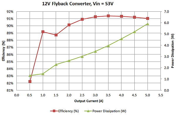
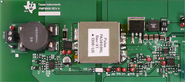
Figure 2 shows the prototype converter’s efficiency, while Figure 3 shows the flyback evaluation board.
 Figure 2 Converter efficiency and
losses dictate package selection and thermal requirements.
 Figure 3 60W flyback evaluation
hardware measures 100mm by 35mm.
Figure 3 60W flyback evaluation
hardware measures 100mm by 35mm.Aid in selecting the proper compensation component values can be investigated here: Compensating isolated power supplies.
This design example covers basic component calculations of a functional CCM flyback design. However, initial estimates often make it necessary to iterate the calculations in order to fine tune it. Still, more detail work is often necessary in areas such as transformer design and control-loop stabilization in order to obtain a well-working, optimized flyback.
Check out TI’s Power Tips blog series on Power House.
Also see:
- Power Tips #76: Flyback converter design considerations
- Quasiresonant flyback converter easily charges energy-storage capacitors
- How to design a flyback converter as a front-end for a two-stage LED driver
- HV flyback converter improves efficiency
Previously published on EDN.com.