-
How a tiny isolated DC/DC module is enabling higher power density
How a tiny isolated DC/DC module is enabling higher power density
Bethlehem Defar and German Aguirre
Introduction
One way to optimize an automotive or industrial design is to reduce the size of the power-supply unit, which can result in system-level cost savings by requiring less physical material and of course fewer discrete components.
Isolated bias-supply solutions such as push-pull and flyback converters have traditionally required heavy, bulky transformers that are prone to vibrations, necessitating a complicated design layout. The design of isolated bias-supply solutions with external transformers also affects performance efficiency and can lead to high radiated electromagnetic interference (EMI).
Breakthroughs in transformer design have allowed integrated circuit designers to fully integrate a transformer and silicon into one package, reducing the isolated DC/DC power supply height and size significantly. The end user obtains a tiny, lightweight isolated power module enabling high power density without having to design a transformer or compromise system performance.
In this article, I’ll describe the basic functionality of three automotive and industrial applications, the importance of the isolated DC/DC power supply to this functionality, and how the new UCC33420-Q1 power module from Texas Instruments can help you to design an effective isolated DC/DC power supply.
Isolated DC/DC power supply in BMS
The main function of a battery management system (BMS) is to monitor pack voltage, pack current and cell voltage. Monitoring high-voltage battery (>60V) leakage current and isolation resistance between the bus and chassis ground is required to comply with safety standards. An isolated DC/DC power supply is present in the high-voltage and isolation diagnosis subsystem within the BMS, providing isolated power to digital isolators and current sensors.
The isolated DC/DC power-supply input gets a 5V supply from the safety power-management integrated circuit and provides 5V of output power to digital isolators, voltage/current sensors or analog-to-digital converters on the high-voltage side in a battery disconnect unit application, as illustrated in Figure 1.
In an intelligent battery junction box using a single voltage, current and insulation resistance monitor, the isolated DC/DC power supply provides an output voltage of 5V to the battery monitor. Advancements in integrated transformer technology occupy less printed circuit board area compared to other push-pull discrete solutions, optimizing power density, reducing system bill-of-materials (BOM) count, and accelerating time to market.
 Figure 1 Battery disconnect unit system
block diagram
Figure 1 Battery disconnect unit system
block diagramEV charging
As the move toward vehicle electrification grows, the need for affordability and reduced charging time increases. Reducing the size of electric vehicle (EV) charging power modules can provide efficiency and reduce overall system cost.
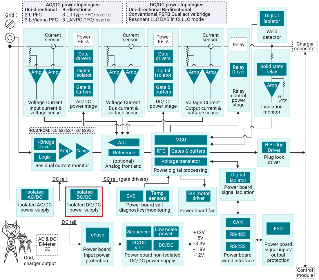
As shown in Figure 2, an EV charging station includes data communication interfaces such as Controller Area Network, RS-485 and isolated amplifiers for voltage and current sensing, which all require isolated DC/DC power. To decrease charging times, there has to be an increase in power output, which can increase overall system size. The UCC33420-Q1’s small footprint and high efficiency can help you design a more efficient isolated power-supply system while reducing overall board space. It is possible to eliminate the number of external components by as much as 50% while supporting the high voltages from AC input lines.
 Figure 2 EV charging station system
block diagram
Figure 2 EV charging station system
block diagramPLC I/O modules
As shown in Figure 3, high-performance programmable logic controller (PLC) systems include several modules in a small space. These PLC systems use centralized input/output (I/O) modules to communicate with sensors, solenoids and valves. The isolated bias supply in a PLC system must be small in size, have tight output-voltage regulation, and be able to mitigate EMI and electromagnetic compatibility. High power density and output-voltage accuracy are also typical requirements.
The UCC33420-Q1’s ability to deliver 1.5W of output power in a 4mm-by-5mm very small outline no-lead package enables this device to power multiple integrated circuits. The UCC33420-Q1 can provide 5V and 3.3V output voltages with accuracy <±3% at VIN 3V to 3.6V and 4.5V to 5.5V, without the need for a post regulator or low-dropout regulator.
 Figure 3 PLC voltage and current output
module block diagram
Figure 3 PLC voltage and current output
module block diagramConclusion
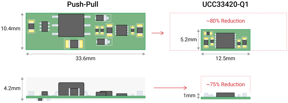
Within the realm of transformer design, the UCC33420-Q1 delivers over 8.5 times higher power density than discrete transformer solutions with the same output power levels. Other innovations over discrete transformer solutions include a reduction in solution size by >89%, a reduction in height by >75%, and a reduction in BOM count by half. Figure 4 compares the size of the UCC33420-Q1 to a push-pull converter.
 Figure 4 UCC33420-Q1 isolated DC/DC
module vs. a traditional push-pull converter
Figure 4 UCC33420-Q1 isolated DC/DC
module vs. a traditional push-pull converterThe UCC33420-Q1 integrates an isolation power transformer, primary- and secondary-side bridges, and control logic into one package, enabling you to meet the demand for smaller and lighter automotive and industrial applications.
The UCC33420-Q1 is designed with an EMI-optimized transformer with 3pF of primary-to-secondary capacitance that can meet Comité International Spécial des Perturbations Radioélectriques (CISPR) 32 compliance without the use of an EMI filter. The device can also meet the CISPR 25 standard with fewer components and a simpler filter design.
Additional resources
- Download the datasheet to learn more about the UCC33420-Q1
- Check out TI’s Isolated DC/DC converters and modules page.
IMPORTANT NOTICE AND DISCLAIMER
TI PROVIDES TECHNICAL AND RELIABILITY DATA (INCLUDING DATASHEETS), DESIGN RESOURCES (INCLUDING REFERENCE DESIGNS), APPLICATION OR OTHER DESIGN ADVICE, WEB TOOLS, SAFETY INFORMATION, AND OTHER RESOURCES “AS IS” AND WITH ALL FAULTS, AND DISCLAIMS ALL WARRANTIES, EXPRESS AND IMPLIED, INCLUDING WITHOUT LIMITATION ANY IMPLIED WARRANTIES OF MERCHANTABILITY, FITNESS FOR A PARTICULAR PURPOSE OR NON-INFRINGEMENT OF THIRD PARTY INTELLECTUAL PROPERTY RIGHTS.
These resources are intended for skilled developers designing with TI products. You are solely responsible for (1) selecting the appropriate TI products for your application, (2) designing, validating and testing your application, and (3) ensuring your application meets applicable standards, and any other safety, security, or other requirements. These resources are subject to change without notice. TI grants you permission to use these resources only for development of an application that uses the TI products described in the resource. Other reproduction and display of these resources is prohibited. No license is granted to any other TI intellectual property right or to any third party intellectual property right. TI disclaims responsibility for, and you will fully indemnify TI and its representatives against, any claims, damages, costs, losses, and liabilities arising out of your use of these resources.
TI’s products are provided subject to TI’s Terms of Sale (www.ti.com/legal/termsofsale.html) or other applicable terms available either on ti.com or provided in conjunction with such TI products. TI’s provision of these resources does not expand or otherwise alter TI’s applicable warranties or warranty disclaimers for TI products.
Mailing Address: Texas Instruments, Post Office Box 655303, Dallas, Texas 75265
Copyright © 2024, Texas Instruments Incorporated