SWAS035C September   2016  – May 2021 CC3220R , CC3220S , CC3220SF

PRODUCTION DATA  

  1. Features
  2. Applications
  3. Description
  4. Functional Block Diagrams
  5. Revision History
  6. Device Comparison
    1. 6.1 Related Products
  7. Terminal Configuration and Functions
    1. 7.1 Pin Diagram
    2. 7.2 Pin Attributes and Pin Multiplexing
      1. 7.2.1 Pin Descriptions
    3. 7.3 Signal Descriptions
      1. 7.3.1 Signal Descriptions
    4. 7.4 Pin Multiplexing
    5. 7.5 Drive Strength and Reset States for Analog and Digital Multiplexed Pins
    6. 7.6 Pad State After Application of Power to Chip But Before Reset Release
    7. 7.7 Connections for Unused Pins
  8. Specifications
    1. 8.1  Absolute Maximum Ratings
    2. 8.2  ESD Ratings
    3. 8.3  Power-On Hours (POH)
    4. 8.4  Recommended Operating Conditions
    5. 8.5  Current Consumption Summary (CC3220R, CC3220S)
    6. 8.6  Current Consumption Summary (CC3220SF)
    7. 8.7  TX Power and IBAT versus TX Power Level Settings
    8. 8.8  Brownout and Blackout Conditions
    9. 8.9  Electrical Characteristics (3.3 V, 25°C)
    10. 8.10 WLAN Receiver Characteristics
    11. 8.11 WLAN Transmitter Characteristics
    12. 8.12 WLAN Filter Requirements
      1. 8.12.1 WLAN Filter Requirements
    13. 8.13 Thermal Resistance Characteristics
      1. 8.13.1 Thermal Resistance Characteristics for RGK Package
    14. 8.14 Timing and Switching Characteristics
      1. 8.14.1 Power Supply Sequencing
      2. 8.14.2 Device Reset
      3. 8.14.3 Reset Timing
        1. 8.14.3.1 nRESET (32-kHz Crystal)
        2. 8.14.3.2 First-Time Power-Up and Reset Removal Timing Requirements (32-kHz Crystal)
        3. 8.14.3.3 nRESET (External 32-kHz)
          1. 8.14.3.3.1 First-Time Power-Up and Reset Removal Timing Requirements (External 32-kHz)
      4. 8.14.4 Wakeup From HIBERNATE Mode
      5. 8.14.5 Clock Specifications
        1. 8.14.5.1 Slow Clock Using Internal Oscillator
          1. 8.14.5.1.1 RTC Crystal Requirements
        2. 8.14.5.2 Slow Clock Using an External Clock
          1. 8.14.5.2.1 External RTC Digital Clock Requirements
        3. 8.14.5.3 Fast Clock (Fref) Using an External Crystal
          1. 8.14.5.3.1 WLAN Fast-Clock Crystal Requirements
        4. 8.14.5.4 Fast Clock (Fref) Using an External Oscillator
          1. 8.14.5.4.1 External Fref Clock Requirements (–40°C to +85°C)
      6. 8.14.6 Peripherals Timing
        1. 8.14.6.1  SPI
          1. 8.14.6.1.1 SPI Master
            1. 8.14.6.1.1.1 SPI Master Timing Parameters
          2. 8.14.6.1.2 SPI Slave
            1. 8.14.6.1.2.1 SPI Slave Timing Parameters
        2. 8.14.6.2  I2S
          1. 8.14.6.2.1 I2S Transmit Mode
            1. 8.14.6.2.1.1 I2S Transmit Mode Timing Parameters
          2. 8.14.6.2.2 I2S Receive Mode
            1. 8.14.6.2.2.1 I2S Receive Mode Timing Parameters
        3. 8.14.6.3  GPIOs
          1. 8.14.6.3.1 GPIO Output Transition Time Parameters (Vsupply = 3.3 V)
            1. 8.14.6.3.1.1 GPIO Output Transition Times (Vsupply = 3.3 V) (1) (1)
          2. 8.14.6.3.2 GPIO Output Transition Time Parameters (Vsupply = 1.85 V)
            1. 8.14.6.3.2.1 GPIO Output Transition Times (Vsupply = 1.85 V) (1) (1)
          3. 8.14.6.3.3 GPIO Input Transition Time Parameters
            1. 8.14.6.3.3.1 GPIO Input Transition Time Parameters'
        4. 8.14.6.4  I2C
          1. 8.14.6.4.1 I2C Timing Parameters (1)
        5. 8.14.6.5  IEEE 1149.1 JTAG
          1. 8.14.6.5.1 JTAG Timing Parameters
        6. 8.14.6.6  ADC
          1. 8.14.6.6.1 ADC Electrical Specifications
        7. 8.14.6.7  Camera Parallel Port
          1. 8.14.6.7.1 Camera Parallel Port Timing Parameters
        8. 8.14.6.8  UART
        9. 8.14.6.9  SD Host
        10. 8.14.6.10 Timers
  9. Detailed Description
    1. 9.1 Arm® Cortex®-M4 Processor Core Subsystem
    2. 9.2 Wi-Fi Network Processor Subsystem
      1. 9.2.1 WLAN
      2. 9.2.2 Network Stack
    3. 9.3 Security
    4. 9.4 Power-Management Subsystem
      1. 9.4.1 VBAT Wide-Voltage Connection
      2. 9.4.2 Preregulated 1.85-V Connection
    5. 9.5 Low-Power Operating Mode
    6. 9.6 Memory
      1. 9.6.1 External Memory Requirements
      2. 9.6.2 Internal Memory
        1. 9.6.2.1 SRAM
        2. 9.6.2.2 ROM
        3. 9.6.2.3 Flash Memory
        4. 9.6.2.4 Memory Map
    7. 9.7 Restoring Factory Default Configuration
    8. 9.8 Boot Modes
      1. 9.8.1 Boot Mode List
  10. 10Applications, Implementation, and Layout
    1. 10.1 Application Information
      1. 10.1.1 Typical Application —CC3220x Wide-Voltage Mode
      2. 10.1.2 Typical Application Schematic—CC3220x Preregulated, 1.85-V Mode
    2. 10.2 PCB Layout Guidelines
      1. 10.2.1 General PCB Guidelines
      2. 10.2.2 Power Layout and Routing
        1. 10.2.2.1 Design Considerations
      3. 10.2.3 Clock Interfaces
      4. 10.2.4 Digital Input and Output
      5. 10.2.5 RF Interface
  11. 11Device and Documentation Support
    1. 11.1 Development Tools and Software
    2. 11.2 Firmware Updates
    3. 11.3 Device Nomenclature
    4. 11.4 Documentation Support
    5. 11.5 Support Resources
    6. 11.6 Trademarks
    7. 11.7 Electrostatic Discharge Caution
    8. 11.8 Export Control Notice
    9. 11.9 Glossary
  12. 12Mechanical, Packaging, and Orderable Information
    1. 12.1 Packaging Information

Brownout and Blackout Conditions

The device enters a brownout condition when the input voltage drops below Vbrownout (see Figure 8-4 and Figure 8-5). This condition must be considered during design of the power supply routing, especially when operating from a battery. High-current operations, such as a TX packet or any external activity (not necessarily related directly to networking) can cause a drop in the supply voltage, potentially triggering a brownout condition. The resistance includes the internal resistance of the battery, the contact resistance of the battery holder (four contacts for 2× AA batteries), and the wiring and PCB routing resistance.

Note:

When the device is in HIBERNATE state, brownout is not detected. Only blackout is in effect during HIBERNATE state.

GUID-169255A0-9C8B-4BD2-82DC-74F5CA809AEF-low.pngFigure 8-4 Brownout and Blackout Levels (1 of 2)
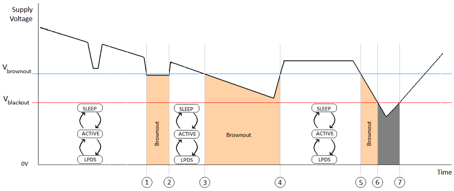
GUID-A0D0A2F6-A279-4D62-90FC-1E4F0A79E8CA-low.pngFigure 8-5 Brownout and Blackout Levels (2 of 2)

In the brownout condition, all sections of the device (including the 32-kHz RTC) shut down except for the Hibernate module, which remains on. The current in this state can reach approximately 400 µA. The blackout condition is equivalent to a hardware reset event in which all states within the device are lost.

Table 8-1 lists the brownout and blackout voltage levels.

Table 8-1 Brownout and Blackout Voltage Levels
CONDITIONVOLTAGE LEVELUNIT
Vbrownout2.1V
Vblackout1.67V