SWAU134 September 2024 CC3301MOD
2.2.4 JTAG Headers
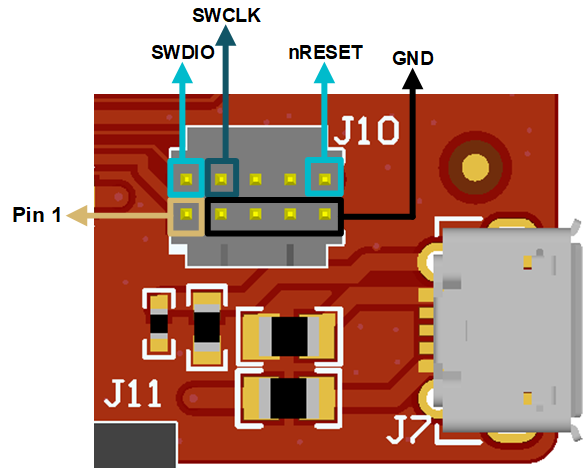
The BP-CC33X1MOD was designed with two headers (J10, and J11) for the SWD interface with the XDS110 debug probe. The signal assignment for these headers are described in the figures and tables below.
The main JTAG interface for the board is via the LP-XDS110ET that is connected to the 20-pin header (J11). An XDS110 debug probe can also interface with this board via a 10-pin header (J10), however, this header is not populated with the default kit.
 Figure 2-4 ARM 10-Pin JTAG Connector (J10)
Table 2-5 ARM 10-Pin JTAG Connector (J10) Assignment
| Pin | Signal Name | Description |
|---|---|---|
| J10.1 | VCC_BRD_1V8 | 1.8V supply for a reference voltage to the connector |
| J10.2 | SWDIO | Serial wire data in/out |
| J10.4 | SWCLK | Serial wire clock |
| J10.10 | RESET_1V8 | nReset (Enable line for CC33X1MOD) |
| J10.3, J10.5, J10.7, J10.9 | GND | Board ground |
 Figure 2-5 20 pin LP-XDS110 Connector (J11)
Table 2-6 20 Pin LP-XDS110 Connector (J11) Assignment
| Pin | Signal Name | Description |
|---|---|---|
| J11.6 | SWCLK | Serial wire clock |
| J11.8 | SWDIO | Serial wire data in/out |
| J11.10 | RESET_1V8 | nReset (Enable line for the CC33X1MOD) |
| J11.12 | UART_TX_1V8 | The CC33X1MOD UART TX to host for BLE host controller interface |
| J11.14 | UART_RX_1V8 | The CC33X1MOD UART RX from host for BLE host controller interface |
| J11.16 | VCC_BRD_1V8 | 1.8V supply for a reference voltage to connector |
| J11.18 | VCC_BRD_5V | 5V supply to BP-CC33X1MOD from LP-XDS110ET |
| J11.1, J11.7, J11.13, J11.19, J11.20 | GND | Board ground |