SWAU134 September   2024 CC3301MOD


  1.   1
  2.   Description
  3.   Features
  4. 1Evaluation Module Overview
    1. 1.1 Introduction
    2. 1.2 Kit Contents
    3. 1.3 Specification
    4. 1.4 Device Information
  5. 2Hardware
    1. 2.1 Hardware Features
    2. 2.2 Connector and Jumper Descriptions
      1. 2.2.1 LED Indicators
      2. 2.2.2 Jumper Settings
      3. 2.2.3 BoosterPack Header Assignment
      4. 2.2.4 JTAG Headers
    3. 2.3 Power
      1. 2.3.1 Measure the CC33X1MOD Current Draw
        1. 2.3.1.1 Low Current Measurement (LPDS)
        2. 2.3.1.2 Active Current Measurement
    4. 2.4 Clocking
    5. 2.5 Performing Conducted Testing
  6. 3Implementation Results
    1. 3.1 Evaluation Setups
      1. 3.1.1 MCU and RTOS
      2. 3.1.2 Processor and Linux
      3. 3.1.3 Standalone RF Testing
        1. 3.1.3.1 Radio Tool BP-CC33X1MOD Hardware Setup
  7. 4Hardware Design Files
    1. 4.1 Schematics
    2. 4.2 PCB Layouts
    3. 4.3 Bill of Materials (BOM)
  8. 5Additional Information
    1. 5.1 Trademarks

Features

  • CC3301MOD Wi-Fi 6® and Bluetooth Low Energy combo device
  • Two 20-pin stackable connectors (BoosterPack Standard)
  • Onboard chip dual-band antenna
  • SMA/U.FL connector for conducted RF testing
  • Power from onboard dual rail (3.3V and 1.8V) LDO using USB or LaunchPad™
  • Three-level shifters for voltage translation (3.3V to 1.8V)
  • JTAG header pins for SWD interface with XDS110 or LP-XDS110ET
  • Jumper for current measurement on both power supplies (3.3V and 1.8V) with provision to mount 0.1-ohm (0603) resistors for measurement with a voltmeter
  • 32kHz oscillator for lower power evaluation
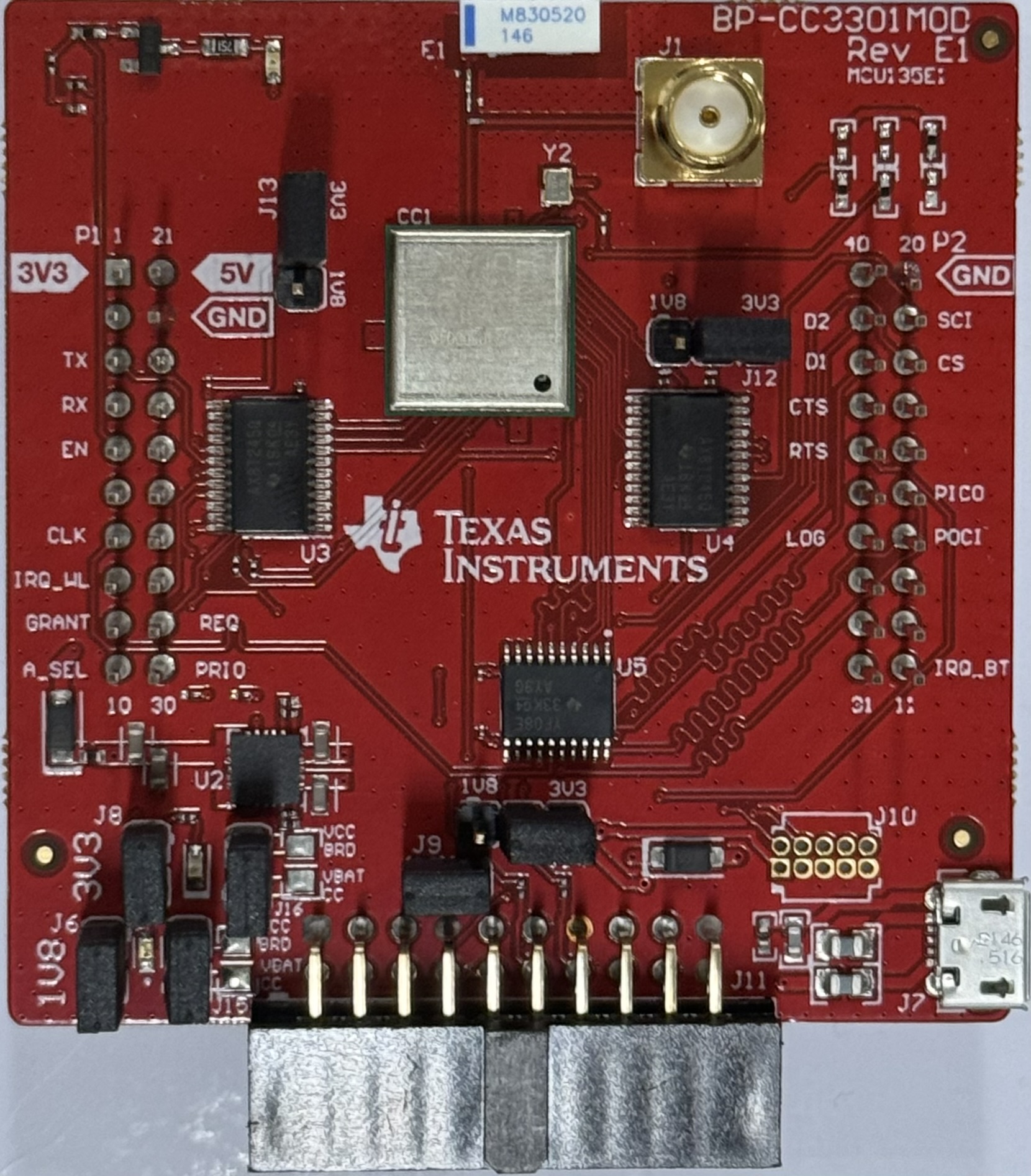
CC3301MOD