SWCS133E September 2015 – October 2024 TPS65094
PRODUCTION DATA
- 1
- 1 Features
- 2 Applications
- 3 Description
- 4 Device Options
- 5 Pin Configuration and Functions
-
6 Specifications
- 6.1 Absolute Maximum Ratings
- 6.2 ESD Ratings
- 6.3 Recommended Operating Conditions
- 6.4 Thermal Information
- 6.5 Electrical Characteristics: Total Current Consumption
- 6.6 Electrical Characteristics: Reference and Monitoring System
- 6.7 Electrical Characteristics: Buck Controllers
- 6.8 Electrical Characteristics: Synchronous Buck Converters
- 6.9 Electrical Characteristics: LDOs
- 6.10 Electrical Characteristics: Load Switches
- 6.11 Digital Signals: I2C Interface
- 6.12 Digital Input Signals (LDOLS_EN, SWA1_EN, THERMTRIPB, PMICEN, SLP_S3B, SLP_S4B, SLP_S0B)
- 6.13 Digital Output Signals (IRQB, RSMRSTB, PCH_PWROK, PROCHOT)
- 6.14 Timing Requirements
- 6.15 Switching Characteristics
- 6.16 Typical Characteristics
-
7 Detailed Description
- 7.1 Overview
- 7.2 Functional Block Diagram
- 7.3 Feature Description
- 7.4 Device Functional Modes
- 7.5 Programming
- 7.6
Register Maps
- 7.6.1 55
- 7.6.2 VENDORID: PMIC Vendor ID Register (offset = 00h) [reset = 0010 0010]
- 7.6.3 DEVICEID: PMIC Device and Revision ID Register (offset = 01h) [reset = OTP Dependent]
- 7.6.4 IRQ: PMIC Interrupt Register (offset = 02h) [reset = 0000 0000]
- 7.6.5 IRQ_MASK: PMIC Interrupt Mask Register (offset = 03h) [reset = 1111 1111]
- 7.6.6 PMICSTAT: PMIC Status Register (offset = 04h) [reset = 0000 0000]
- 7.6.7 OFFONSRC: PMIC Power Transition Event Register (offset = 05h) [reset = 0000 0000]
- 7.6.8 BUCK1CTRL: BUCK1 Control Register (offset = 20h) [reset = 0011 1000]
- 7.6.9 BUCK2CTRL: BUCK2 Control Register (offset = 21h) [reset = 0000 0000]
- 7.6.10 BUCK3CTRL: BUCK3 Control Register (offset = 23h) [reset = 0001 0001]
- 7.6.11 BUCK4CTRL: BUCK4 Control Register (offset = 25h) [reset = OTP Dependent]
- 7.6.12 BUCK5CTRL: BUCK5 Control Register (offset = 26h) [reset = OTP Dependent]
- 7.6.13 BUCK6CTRL: BUCK6 Control Register (offset = 27h) [reset = 0011 1101]
- 7.6.14 DISCHCNT1: Discharge Control1 Register (offset = 40h) [reset = 0101 0101]
- 7.6.15 DISCHCNT2: Discharge Control2 Register (offset = 41h) [reset = 0101 0101]
- 7.6.16 DISCHCNT3: Discharge Control3 Register (offset = 42h) [reset = 0000 0101]
- 7.6.17 POK_DELAY: PCH_PWROK Delay Register (offset = 43h) [reset = 0000 0111]
- 7.6.18 FORCESHUTDN: Force Emergency Shutdown Control Register (offset = 91h) [reset = 0000 0000]
- 7.6.19 BUCK4VID: BUCK4 VID Register (offset = 94h) [reset = 0010 1111]
- 7.6.20 BUCK5VID: BUCK5 VID Register (offset = 96h) [reset = 0100 1011]
- 7.6.21 BUCK6VID: BUCK6 VID Register (offset = 98h) [reset = OTP Dependent]
- 7.6.22 LDOA2VID: LDOA2 VID Register (offset = 9Ah) [reset = OTP Dependent]
- 7.6.23 LDOA3VID: LDOA3 VID Register (offset = 9Bh) [reset = OTP Dependent]
- 7.6.24 VR_CTRL1: BUCK1-3 Control Register (offset = 9Ch) [reset = OTP Dependent]
- 7.6.25 VR_CTRL2: VR Enable Register (offset = 9Eh) [reset = 0000 0000]
- 7.6.26 VR_CTRL3: VR Enable/Disable Register (offset = 9Fh) [reset = OTP Dependent]
- 7.6.27 GPO_CTRL: GPO Control Register (offset = A1h) [reset = 0010 0000]
- 7.6.28 PWR_FAULT_MASK1: VR Power Fault Mask1 Register (offset = A2h) [reset = 1100 0000]
- 7.6.29 PWR_FAULT_MASK2: VR Power Fault Mask2 Register (offset = A3h) [reset = 0011 0111]
- 7.6.30 DISCHCNT4: Discharge Control4 Register (offset = ADh) [reset = 0110 0001]
- 7.6.31 LDOA1CTRL: LDOA1 Control Register (offset = AEh) [reset = OTP Dependent]
- 7.6.32 PG_STATUS1: Power Good Status1 Register (offset = B0h) [reset = 0000 0000]
- 7.6.33 PG_STATUS2: Power Good Status2 Register (offset = B1h) [reset = 0000 0000]
- 7.6.34 TEMPHOT: Temperature Hot Status Register (offset = B5h) [reset = 0000 0000]
-
8 Application and Implementation
- 8.1 Typical Application
- 8.2 Specific Application for TPS650944
- 8.3 Dos and Don'ts
- Power Supply Recommendations
- 8.4 Layout
- 9 Device and Documentation Support
- 10Revision History
- 11Mechanical, Packaging, and Orderable Information
7.3.3.2 Converter Overview
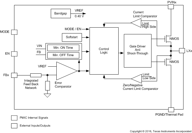
The PMIC synchronous step-down DC-DC converters include a unique hysteretic PWM control scheme which enables a high switching frequency converter, excellent transient and AC load regulation, as well as operation with cost-competitive external components. The controller topology supports forced PWM mode as well as power-save mode operation. Power-save mode operation, or PFM mode, reduces the quiescent current consumption and ensures high conversion efficiency at light loads by skipping switch pulses. In forced PWM mode, the device operates on a quasi-fixed frequency, avoids pulse skipping, and allows filtering of the switch noise by external filter components. The PMIC device offers fixed output voltage options featuring smallest solution size by using only three external components per converter.
A significant advantage of PMIC compared to other hysteretic PWM controller topologies is the excellent capability of the AC load transient regulation. When the output voltage falls below the threshold of the error comparator, a switch pulse is initiated, and the high-side switch is turned on. The high-side switch remains turned on until a minimum ON-time of tONmin expires and the output voltage trips the threshold of the error comparator or the inductor current reaches the high-side switch current limit. When the high-side switch turns off, the low-side switch rectifier is turned on and the inductor current ramps down until the high-side switch turns on again or the inductor current reaches zero. In forced PWM mode operation, negative inductor current is allowed to enable continuous conduction mode even at no load condition.
 Figure 7-4 Converter Block Diagram