SWCU192 November 2021 CC1312R7 , CC1352P7 , CC2652P7 , CC2652R7
9.2.1.3 Cache Mode
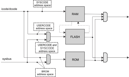
In cache mode, the RAM block functions as an 8K 4-way random replacement cache for the FLASH block (see Figure 9-5). The GPRAM space is not available in cache mode.
The cache support is only available for CPU accesses to the FLASH SYSCODE address space. System bus accesses to the FLASH block and CPU accesses to the FLASH USERCODE address space are routed directly to the FLASH block.
 Figure 9-5 VIMS Module in Cache Mode
In cache mode, all CPU accesses to the FLASH SYSCODE address space are directed to the cache first. The cache looks up the input address in the internal tag RAM to determine whether the access is a cache hit or a cache miss.
In the case of a cache miss, the access is forwarded to the FLASH block. The response from the FLASH block is routed back to the cache, then the cache is updated.
In the case of a cache hit, the data is fetched directly from the cache RAM.
The cache also contains a line buffer because the cache RAM word size is 64 bits. The objective of the line buffer is to prevent refetching the 32-bit part of the data that has already been fetched (but not used) in the previous access. The line buffer prevents both TAG and CACHE lookup if the data is already in the line buffer.
The cache line buffer is cleared as a part of the invalidation scheme.