SWRA640H December   2018  – May 2024 CC1310 , CC1312R , CC1314R10 , CC1350 , CC1352P , CC1352R , CC1354P10 , CC1354R10 , CC2620 , CC2630 , CC2640 , CC2640R2F , CC2640R2F-Q1 , CC2642R , CC2642R-Q1 , CC2650 , CC2652P , CC2652R , CC2652R7 , CC2652RB , CC2652RSIP , CC2674P10 , CC2674R10


  1.   1
  2.   Abstract
  3.   Trademarks
  4. Reference Design
    1. 1.1 Sub-1GHz LaunchPads
      1. 1.1.1 LAUNCHXL-CC1310
      2. 1.1.2 LAUNCHXL-CC1312R
    2. 1.2 2.4GHz LaunchPads
      1. 1.2.1 LAUNCHXL-CC2640R2
      2. 1.2.2 LAUNCHXL-CC26x2R
      3. 1.2.3 LP-CC26x1
    3. 1.3 Dual-Band LaunchPads
      1. 1.3.1 LAUNCHXL-CC1350EU/US
      2. 1.3.2 LAUNCHXL-CC1350-4
      3. 1.3.3 LAUNCHXL-CC1352R
      4. 1.3.4 LAUNCHXL-CC1352P1
      5. 1.3.5 LAUNCHXL-CC1352P-2
      6. 1.3.6 LAUNCHXL-CC1352P-4
      7. 1.3.7 LP-CC1352P7-1
      8. 1.3.8 LP-CC1352P7-4
      9. 1.3.9 LP-EM-CC1354P10-6
    4. 1.4 Reference Design Overview
  5. Front-End Configurations
    1. 2.1 Overview of Front-end Configurations
    2. 2.2 Configuring the Front-End Mode
    3. 2.3 CC13xx Single-Ended Mode
      1. 2.3.1 Single-Ended Modes
      2. 2.3.2 Single-Ended TX-Only
      3. 2.3.3 Single-Ended RX-Only
      4. 2.3.4 Single-Ended Modes - 2.4GHz
    4. 2.4 CC26xx Single-End Mode
  6. Schematic
    1. 3.1 Schematic Overview
      1. 3.1.1 24/48MHz Crystal
      2. 3.1.2 32.768kHz Crystal
      3. 3.1.3 Balun
      4. 3.1.4 Filter
      5. 3.1.5 RX_TX Pin
      6. 3.1.6 Decoupling Capacitors
      7. 3.1.7 Antenna Components
      8. 3.1.8 RF Shield
      9. 3.1.9 I/O Pins Drive Strength
    2. 3.2 Bootloader Pins
    3. 3.3 AUX Pins
      1. 3.3.1 Reference
      2. 3.3.2 CC26x2/CC13x2 AUX Pins
      3. 3.3.3 CC26x0/CC13x0 AUX Pins
    4. 3.4 JTAG Pins
  7. PCB Layout
    1. 4.1  Board Stack-Up
    2. 4.2  Balun - Sub-1GHz
    3. 4.3  Balun - 2.4GHz
      1. 4.3.1 Recommended Layout and Considerations for 20dBm
    4. 4.4  LC Filter
    5. 4.5  Decoupling Capacitors
    6. 4.6  Placement of Crystal Load Capacitors
    7. 4.7  Current Return Path
    8. 4.8  DC/DC Regulator
    9. 4.9  Antenna Matching Components
    10. 4.10 Transmission Lines
    11. 4.11 Electromagnetic Simulation
  8. Antenna
    1. 5.1 Single-Band Antenna
    2. 5.2 Dual-Band Antenna
      1. 5.2.1 Dual-Band Antenna Match Example: 863-928 MHz and 2.4 GHz
      2. 5.2.2 Dual-Band Antenna Match: 433-510MHz and 2.4GHz
  9. Crystal Tuning
    1. 6.1 CC13xx/CC26xx Crystal Oscillators
    2. 6.2 Crystal Selection
    3. 6.3 Tuning the LF Crystal Oscillator
    4. 6.4 Tuning the HF Oscillator
  10. TCXO Support
    1. 7.1 Hardware
    2. 7.2 Software
    3. 7.3 Example: Usage of TCXO on CC1312R Launchpad
  11. Integrated Passive Component (IPC)
  12. Optimum Load Impedance
  13. 10PA Table
  14. 11Power Supply Configuration
    1. 11.1 Introduction
    2. 11.2 DC/DC Converter Mode
    3. 11.3 Global LDO Mode
    4. 11.4 External Regulator Mode
  15. 12Board Bring-Up
    1. 12.1 Power On
    2. 12.2 RF Test: SmartRF Studio
    3. 12.3 RF Test: Conducted Measurements
      1. 12.3.1 Sensitivity
      2. 12.3.2 Output Power
    4. 12.4 Software Bring-Up
    5. 12.5 Hardware Troubleshooting
      1. 12.5.1 No Link: RF Settings
      2. 12.5.2 No Link: Frequency Offset
      3. 12.5.3 Poor Link: Antenna
      4. 12.5.4 Bluetooth Low Energy: Device Does Advertising But Cannot Connect
      5. 12.5.5 Poor Sensitivity: DCDC Layout
      6. 12.5.6 Poor Sensitivity: Background noise
      7. 12.5.7 High Sleep Power Consumption
  16. 13References
  17. 14Revision History

Balun - Sub-1GHz

It is important to keep the balun as close and symmetrical as possible with regard to the RF ports. Therefore, the trace length from the single ended port to each of the RF pins should be equal to achieve best amplitude and phase balance. For a good balun PCB layout, see Figure 4-2. An unbalance in the balun causes higher harmonic levels, especially at the 2nd and 4th harmonics. Another effect of having an unsymmetrical balun is reduced output power at the single ended side of the balun. Both component values and component placement is important to achieve best possible symmetry in the balun. Amplitude imbalance should be a maximum of 1.5dB and the phase imbalance a maximum of 10°.

To ensure optimal performance it is important to implement the same layout of the balun, match, and filter as in the reference design. Changing the placement of these parts might require tuning on the component values to obtain the desired performance. Tuning requires advanced RF skills and the proper equipment.

There must be an uninterrupted and solid ground plane under all the RF components, stretching from the antenna and all the way back to the ground vias in the chip exposed ground pad (EGP). There must not be any traces under the RF path.
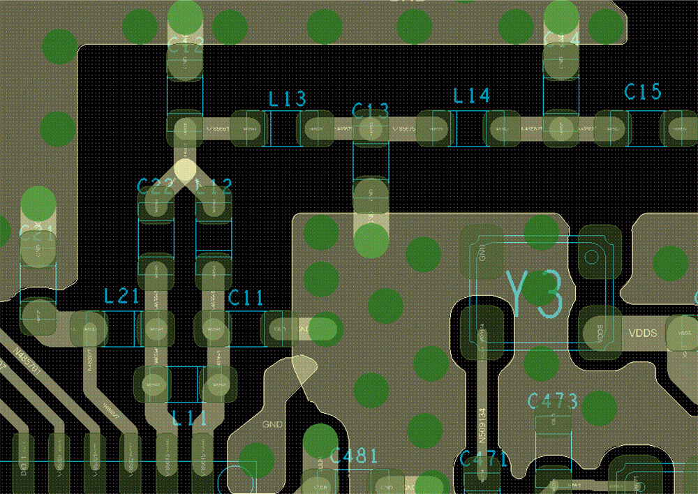
CC1354P10-6 CC1312R Balun and LC Filter PCB LayoutFigure 4-2 CC1312R Balun and LC Filter PCB Layout