SWRA672 May   2020 AWR6843AOP , IWR6843AOP


  1.   Thermal Design Guide for Antenna on Package mmWave Sensor
    1.     Trademarks
    2. 1 Introduction
    3. 2 mmWave AoP package
      1. 2.1 Thermal Characteristics of the Package
    4. 3 Salient features of AoP EVM
      1. 3.1 Thermal Challenges in Dissipating the Heat
    5. 4 Techniques for Mitigating the Heat Dissipation
      1. 4.1 Reduce the System Level Thermal Resistance
      2. 4.2 Board Size Scaling
      3. 4.3 Heatsink Options
        1. 4.3.1 Sheet Metal Heat Sink
        2. 4.3.2 Heat Sink Details
        3. 4.3.3 Mounting Options
        4. 4.3.4 Thermal Characteristics With the Sheet-Metal Heatsink
      4. 4.4 Heatsink with fins
        1. 4.4.1 Thermal Characteristics With the Heatsink
    6. 5 PCB based thermal improvements
      1. 5.1 Thermal via array
    7. 6 Application and Demos
    8. 7 Summary
    9. 8 Acknowledgment
    10. 9 References

mmWave AoP package

The antenna-on-package (AoP) mmWave sensor uses the under-mount silicon attached package, unlike other flip-chip-chip-scale package packages. In this package, die is exposed outside the package and attached to the substrate from the bottom side of the package.
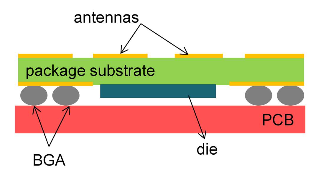
package_image.jpgFigure 1. Under-Mount Silicon Package on a PCB

mmWave sensor package is 0.8 mm pitch, 180 balls, 15 mm x 15 mm dimension. This allows easy assembly and low-cost PCB design. BGA has fully populated balls in the package, which allows greater thermal contact to the PCB and also provides better mechanical and board level reliability for the package catering to automotive and industrial applications.
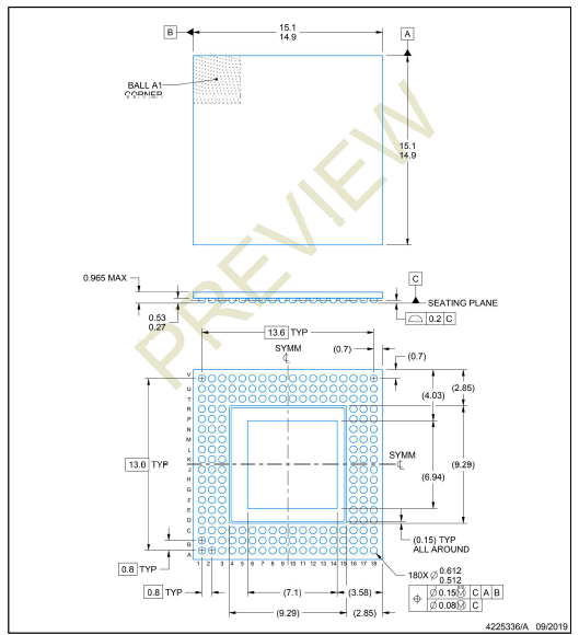
Package_out_line_drawing.pngFigure 2. Package Outline Drawing