SWRA797 September 2024 CC1312PSIP
3.1.1 4-Layer Design
The LP-EM-CC1312PSIP [4.2] is available for evaluation of the CC1312PSIP [4.1] and is a 4-layer design. The function of the LP-EM-CC1312PSIP [4.2] has been shown in Figure 1-3. This is the design that has been tested at FCC test house. LP-EM-CC1312PSIP [4.2] has also been tested at 868MHz to sell the evaluation board in Europe.
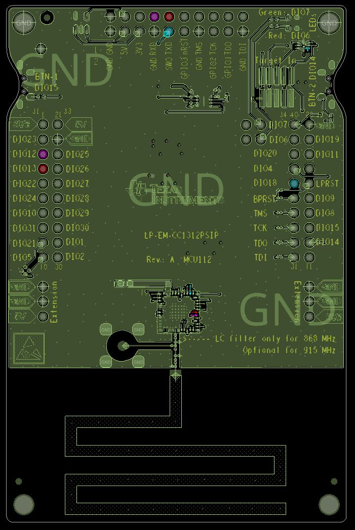
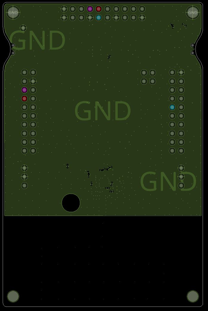
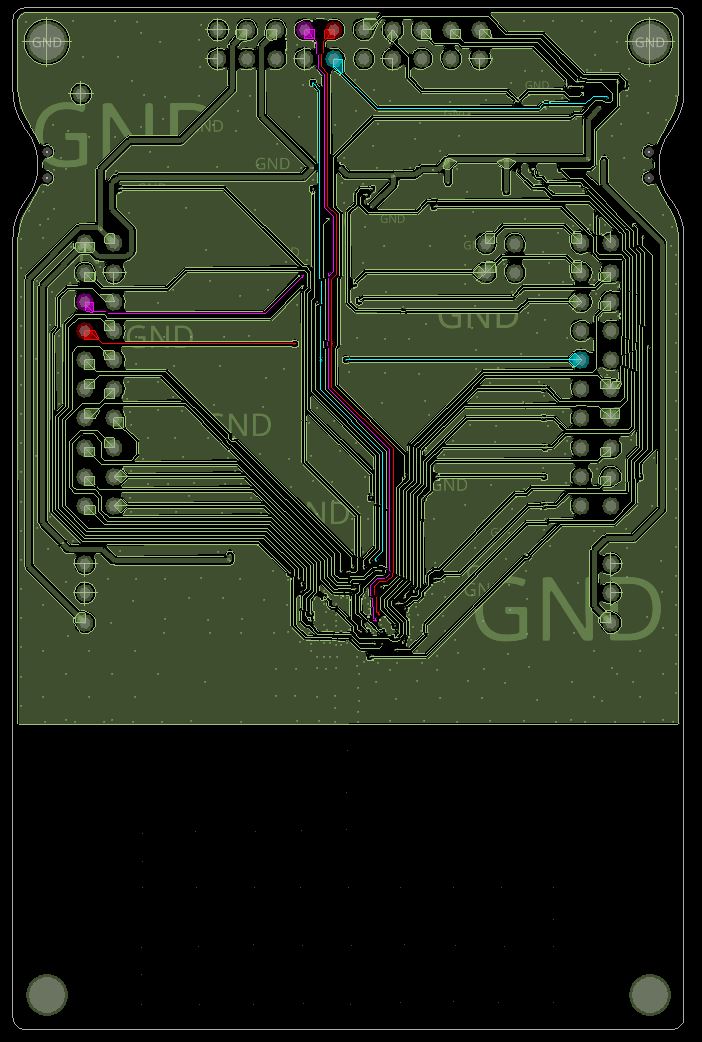
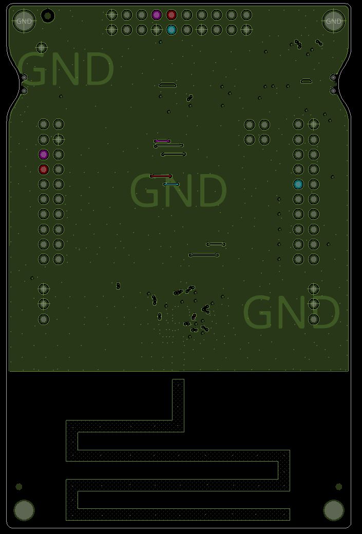
The 4-layer layout has been designed to minimize the emissions from the board. The top layer is the component layer which the CC1312PSIP [4.1] is soldered and assembled, refer to Figure 3-1. Directly underneath the top layer, is the second layer that is mostly the GND layer, refer to Figure 3-2. The third layer is the layer where the majority of the routing is performed, refer to Figure 3-3. The bottom layer there is minimum routing and the majority of this layer is a GND plane, refer to Figure 3-4.
By enclosing the majority of the routing on the third layer, between the GND on the second and fourth layers. The GND layers with the GND vias then form a Faraday cage effect on the majority of the routing performed on the third layer which helps to minimize unwanted emissions from the routing of the signals from the CC1312PSIP [4.1]. As can be seen in Figure 3-1 and Figure 3-4, the routing on the top and bottom layers are kept to a minimum.
A 4-layer design is the preferred choice for a robust and low emission design.
 Figure 3-1 Top Component Layer of the
4-Layer PCB Design
 Figure 3-2 Second Layer of the
4-Layer PCB Design
 Figure 3-3 Third Layer of the 4-Layer
PCB Design
 Figure 3-4 Bottom Layer of the
4-Layer PCB Design