SWRA797 September 2024 CC1312PSIP
3.1.2 2-Layer Design
Since the CC1312PSIP [4.1] has integrated all the components inside the package. The routing requirements to the CC1312PSIP are simplified and this opens up the option to produce a 2-layer PCB design instead of a 4-layer PCB design to save PCB costs.
Since there is only 2 layers of the PCB, the more IO routing inherently decreases the amount of GND on the PCB. Not only does the GND plane reduce, but the Faraday cage effects are also reduced compared to a 4-layer design.
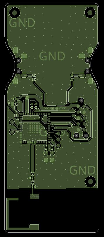
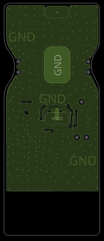
Figure 3-5 shows the top layer of a 2-layer PCB design and Figure 3-6 shows the bottom layer of the 2-layer PCB design. The Faraday cage concept is still tried to be maintained despite having just two layers. Making a 2-layer design is more challenging than making a 4-layer design since the design has greater requirements that a good RF layout concept must be followed. If good RF layout practice is not followed on the end-product, then the unintentional radiated emissions increase which can cause failures at the certified test lab when proving the level of unintentional radiators is within the regulatory limits.
The top layer shown in Figure 3-5 is the component layer with the main routing layer. The bottom layer shown in Figure 3-6 is for minor routing and mostly GND plane layer. The bottom layer which is mostly a GND layer is important for the Faraday cage effects and also to maintain a large GND plane as possible for the antenna.
A smaller GND plane naturally gives a lower antenna efficiency and a smaller bandwidth. This is one of the reasons why there must be as little as possible routing on this layer to maintain a highly efficient antenna for a GND plane size that is much smaller than a quarter-wave. The quarter-wave at 915MHz is 8.2cm so GND planes that are less than this distance have a reduced efficiency and bandwidth. The antenna must see as large as possible GND plane for best antenna efficiency. If the GND plane is effectively divided up due to routing, the antenna efficiency is lower.
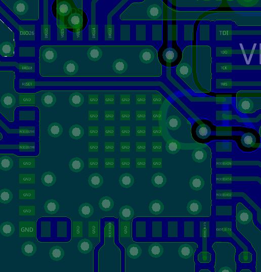
Figure 3-7 shows the top and bottom layer of the 2-layer PCB design directly underneath the CC1312PSIP. The GND vias and the distance between the GND vias are essential to maintain a good Faraday cage effect whilst just having a 2-layer design.
Making a 2-layer design requires more caution in the RF layout stage of the design. By not having a good GND plane or using enough GND vias, then the design has increased emissions. If there is uncertainty or if the previous guidelines cannot be followed, then a 4-layer design can be used.
 Figure 3-5 Top Layer of 2-Layer PCB
Design
 Figure 3-6 Bottom Layer of 2-layer
PCB Design
 Figure 3-7 Top and Bottom Layer of
2-Layer PCB Directly Underneath the CC1312PSIP