SWRA797 September   2024 CC1312PSIP


  1.   1
  2.   Abstract
  3.   Trademarks
  4. 1Introduction
    1. 1.1 RF Function and Frequency Range
    2. 1.2 LP-EM-CC1312PSIP
  5. 2Software – Certified PHYs
    1. 2.1 14dBm Tx and Rx Port
      1. 2.1.1 WB-DSSS
      2. 2.1.2 TI 15.4
      3. 2.1.3 PowerG PHY
      4. 2.1.4 mioty PHY
      5. 2.1.5 WiSun PHY
    2. 2.2 20dBm Tx Port
      1. 2.2.1 WB-DSSS PHY
      2. 2.2.2 TI 15.4 PHY
      3. 2.2.3 PowerG PHY
      4. 2.2.4 mioty PHY
      5. 2.2.5 Wi-SUN PHY
  6. 3Hardware
    1. 3.1 Recommended Layout
      1. 3.1.1 4-Layer Design
      2. 3.1.2 2-Layer Design
      3. 3.1.3 GND Vias
      4. 3.1.4 Maximum Track Length
    2. 3.2 Antennas
      1. 3.2.1 Certified Antennas
      2. 3.2.2 Cross-Linking Certified Antennas
    3. 3.3 Reusing of FCC ID and IC
      1. 3.3.1 Documentation Supplied to the TCB
      2. 3.3.2 Permissive Change Policy
        1. 3.3.2.1 Class 1 Permissive Change (C1PC)
        2. 3.3.2.2 Class 2 Permissive Change (C2PC)
        3. 3.3.2.3 Class 3 Permissive Change (C3PC)
      3. 3.3.3 Changes in the FCC ID or IC
      4. 3.3.4 Re-use of FCC ID and IC Certifications Step-by-Step
    4. 3.4 Recommended Production Testing
  7. 4References

Maximum Track Length

For a 4-layer design, the maximum track length on the top and bottom layers that are outside the Faraday cage can not be longer than 8mm since the majority of the routing can be done on the third layer.

Note: For a 2-layer design, the maximum track length recommendation of 8mm can be difficult to follow since the main routing is done mainly on the top layer. If the tracks on the top layer exceed 8mm in length, then these tracks must have a GND directly underneath on the bottom layer to minimize the unwanted radiation of the long tracks that exceed 8mm.
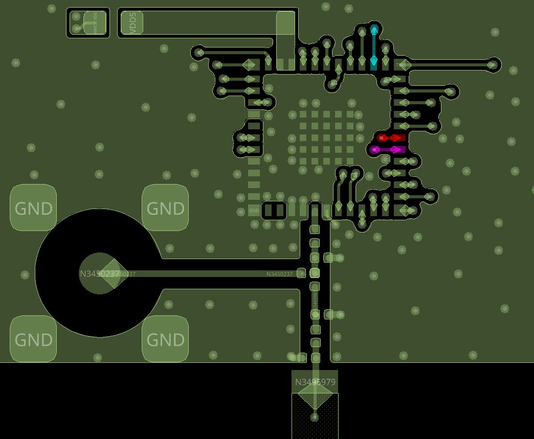
 Maximum Track Length on Top
                    Layer of a 4-Layer PCB and GND Via Placement Figure 3-8 Maximum Track Length on Top Layer of a 4-Layer PCB and GND Via Placement