SWRA824 October 2024 CC1120
3 Causes of Spurious Emissions
Spurious emissions are signals caused by transmitted frequency content that is outside of the carrier frequency band of a transmitter. This can be caused by a SMPS or nearby radio transmitter that could be inadvertently transmitting weak signals on a frequency not assigned to that transmitter. FCC regulations concerning spurious emissions state that if interference is caused by spurious emissions, the operator of the transmitter must take whatever steps are necessary to reduce the spurious emissions as required by FCC regulations.
As mentioned earlier, when a SMPS operates, it outputs a voltage that also has ripple on top of the regulated steady-state DC value. This ripple voltage is composed of one or multiple different frequencies. The frequency composition of this ripple voltage interferes with the frequency output of the transceiver, which results in spurious emissions. This shows up as multiple frequency harmonics outside of the carrier frequency. If the frequency content of a specific frequency is too abundant, it may result in a failing outcome when testing to FCC standards for the band of interest. This is important when observing the output voltage of an SMPS as many different factors can affect it's ripple value and frequency content, resulting in spurious emissions.
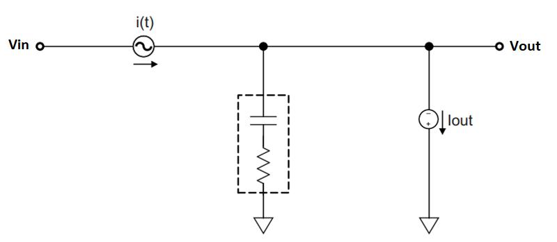
Assuming the simple schematic of the output capacitor in a buck regulator in Figure 3-1, the total voltage ripple output in a buck regulator can be derived.
 Figure 3-1 Schematic for Analytical
Derivation of Output Voltage Waveform
Figure 3-1 Schematic for Analytical
Derivation of Output Voltage WaveformThe total voltage ripple output in a buck regulator can be expressed as (full derivation can be found on Output Ripple Voltage for Buck Switching Regulator (Rev. A) (ti.com)):
Where VC represents the voltage ripple contributing from capacitor-only portion, VR represents the voltage ripple contribution from the resistor-only portion, R represents the resistance value, C represents the capacitance, Fsw represents the switching frequency of the regulator, and D represents the duty cycle. The output capacitor, C, is assumed to have an equivalent series resistance, R (denoted by the components shown in the dotted box in Figure 3-1). This equation reveals the total output ripple is dependent on many factors of the circuit, such as the resistor, capacitor, duty cycle, and switching frequency. This is significant because the frequency composition of the output ripple voltage determines the levels of spurious emissions seen in the frequency spectrum on the antenna. If an engineer decides to change any of these values to better fit an output in their application, it may result in unwanted frequency interference at impermissible levels.