-
AWR1243 Single-Chip 77- and 79-GHz FMCW Transceiver
- 1 Features
- 2 Applications
- 3 Description
- 4 Functional Block Diagram
- 5 Revision History
- 6 Device Comparison
- 7 Terminal Configuration and Functions
-
8 Specifications
- 8.1 Absolute Maximum Ratings
- 8.2 ESD Ratings
- 8.3 Power-On Hours (POH)
- 8.4 Recommended Operating Conditions
- 8.5 Power Supply Specifications
- 8.6 Power Consumption Summary
- 8.7 RF Specification
- 8.8 Thermal Resistance Characteristics for FCBGA Package [ABL0161]
- 8.9
Timing and Switching Characteristics
- 8.9.1 Power Supply Sequencing and Reset Timing
- 8.9.2 Synchronized Frame Triggering
- 8.9.3 Input Clocks and Oscillators
- 8.9.4 Multibuffered / Standard Serial Peripheral Interface (MibSPI)
- 8.9.5 LVDS Interface Configuration
- 8.9.6 General-Purpose Input/Output
- 8.9.7 Camera Serial Interface (CSI)
- 9 Detailed Description
- 10Monitoring and Diagnostics
- 11Applications, Implementation, and Layout
- 12Device and Documentation Support
- 13Mechanical, Packaging, and Orderable Information
- IMPORTANT NOTICE
AWR1243 Single-Chip 77- and 79-GHz FMCW Transceiver
1 Features
- FMCW transceiver
- Integrated PLL, transmitter, receiver, Baseband, and ADC
- 76- to 81-GHz coverage with 4 GHz available bandwidth
- Four receive channels
- Three transmit channels (two can be used simultaneously)
- Ultra-accurate chirp engine based on fractional-N PLL
- TX power: 12 dBm
- RX noise figure:
- 14 dB (76 to 77 GHz)
- 15 dB (77 to 81 GHz)
- Phase noise at 1 MHz:
- –95 dBc/Hz (76 to 77 GHz)
- –93 dBc/Hz (77 to 81 GHz)
- Built-in calibration and self-test
- Built-in firmware (ROM)
- Self-calibrating system across process and temperature
- Host interface
- Control interface with external processor over SPI
- Data interface with external processor over MIPI D-PHY and CSI2 V1.1
- Interrupts for fault reporting
- Functional Safety-Compliant
- Developed for functional safety applications
- Documentation available to aid ISO 26262 functional safety system design up to ASIL-D
- Hardware integrity up to ASIL-B
- Safety-related certification
- ISO 26262 certified upto ASIL B by TUV SUD
- AEC-Q100 qualified
- Device advanced features
- Embedded self-monitoring with no host processor involvement
- Complex baseband architecture
- Embedded interference detection capability
- Power management
- Built-in LDO network for enhanced PSRR
- I/Os support dual voltage 3.3 V/1.8 V
- Clock source
- Supports externally driven clock (square/sine) at 40 MHz
- Supports 40 MHz crystal connection with load capacitors
- Easy hardware design
- 0.65-mm pitch, 161-pin 10.4 mm × 10.4 mm flip chip BGA package for easy assembly and low-cost PCB design
- Small solution size
- Operating Conditions
- Junction temp range: –40°C to 125°C
2 Applications
- Automotive Sensor for measuring range, velocity and angle
- Automated highway driving
- Automatic emergency braking
- Adaptive cruise control
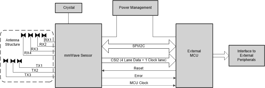
 Figure 2-1 Autonomous Radar Sensor For Automotive Applications
3 Description
The AWR1243 device is an integrated single-chip FMCW transceiver capable of operation in the 76- to 81-GHz band. The device enables unprecedented levels of integration in an extremely small form factor. AWR1243 is an ideal solution for low power, self-monitored, ultra-accurate radar systems in the automotive space.
The AWR1243 device is a self-contained FMCW transceiver single-chip solution that simplifies the implementation of Automotive Radar sensors in the band of 76 to 81 GHz. It is built on TI’s low-power 45-nm RFCMOS process, which enables a monolithic implementation of a 3TX, 4RX system with built-in PLL and ADC converters. Simple programming model changes can enable a wide variety of sensor implementation (Short, Mid, Long) with the possibility of dynamic reconfiguration for implementing a multimode sensor. Additionally, the device is provided as a complete platform solution including TI reference designs, software drivers, sample configurations, API guides, and user documentation.
| PART NUMBER(2) | PACKAGE(1) | BODY SIZE | TRAY / TAPE AND REEL |
|---|---|---|---|
| AWR1243FBIGABLQ1 | FCBGA (161) | 10.4 mm × 10.4 mm | Tray |
| AWR1243FBIGABLRQ1 | Tape and Reel |
4 Functional Block Diagram
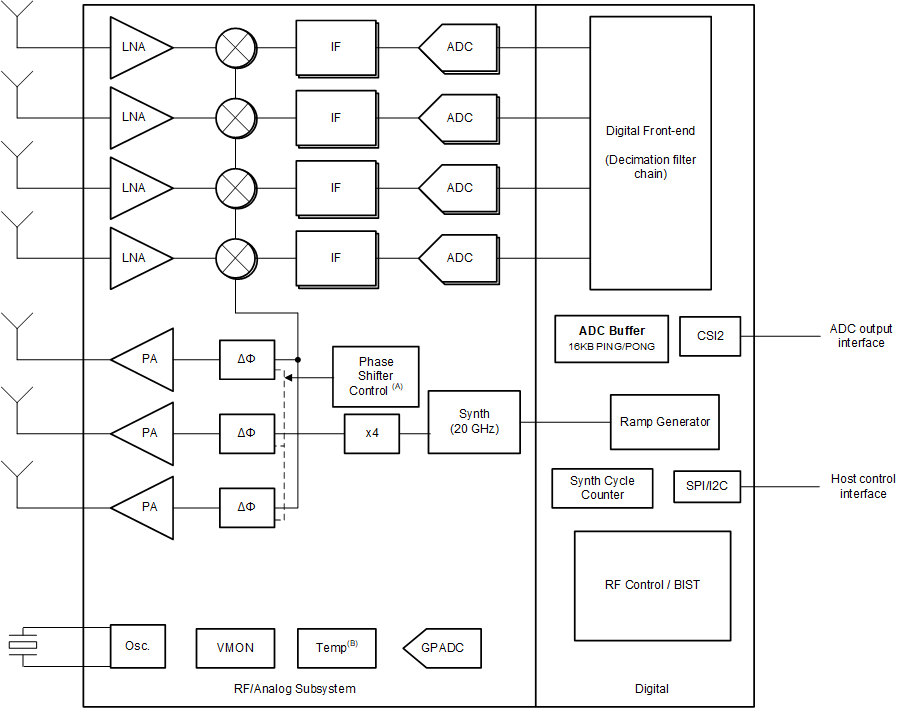
Figure 4-1 shows the functional block diagram of the device.

- 0° / 180° BPM for AWR1243