SWRS188D May 2017 – December 2021 AWR1243
PRODUCTION DATA
- 1 Features
- 2 Applications
- 3 Description
- 4 Functional Block Diagram
- 5 Revision History
- 6 Device Comparison
- 7 Terminal Configuration and Functions
-
8 Specifications
- 8.1 Absolute Maximum Ratings
- 8.2 ESD Ratings
- 8.3 Power-On Hours (POH)
- 8.4 Recommended Operating Conditions
- 8.5 Power Supply Specifications
- 8.6 Power Consumption Summary
- 8.7 RF Specification
- 8.8 Thermal Resistance Characteristics for FCBGA Package [ABL0161]
- 8.9
Timing and Switching Characteristics
- 8.9.1 Power Supply Sequencing and Reset Timing
- 8.9.2 Synchronized Frame Triggering
- 8.9.3 Input Clocks and Oscillators
- 8.9.4 Multibuffered / Standard Serial Peripheral Interface (MibSPI)
- 8.9.5 LVDS Interface Configuration
- 8.9.6 General-Purpose Input/Output
- 8.9.7 Camera Serial Interface (CSI)
- 9 Detailed Description
- 10Monitoring and Diagnostics
- 11Applications, Implementation, and Layout
- 12Device and Documentation Support
- 13Mechanical, Packaging, and Orderable Information
9.3.1.2 Transmit Subsystem
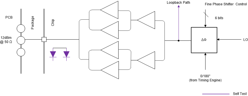
The AWR1243 transmit subsystem consists of three parallel transmit chains, each with independent phase and amplitude control. A maximum of two transmit chains can be operational at the same time, however all three chains can be operated together in a time-multiplexed fashion. The device supports binary phase modulation for MIMO radar and interference mitigation.
Each transmit chain can deliver a maximum of 12 dBm at the antenna port on the PCB. The transmit chains also support programmable backoff for system optimization.
Figure 9-3 describes the transmit subsystem.
 Figure 9-3 Transmit
Subsystem (Per Channel)