SWRS188D May 2017 – December 2021 AWR1243
PRODUCTION DATA
- 1 Features
- 2 Applications
- 3 Description
- 4 Functional Block Diagram
- 5 Revision History
- 6 Device Comparison
- 7 Terminal Configuration and Functions
-
8 Specifications
- 8.1 Absolute Maximum Ratings
- 8.2 ESD Ratings
- 8.3 Power-On Hours (POH)
- 8.4 Recommended Operating Conditions
- 8.5 Power Supply Specifications
- 8.6 Power Consumption Summary
- 8.7 RF Specification
- 8.8 Thermal Resistance Characteristics for FCBGA Package [ABL0161]
- 8.9
Timing and Switching Characteristics
- 8.9.1 Power Supply Sequencing and Reset Timing
- 8.9.2 Synchronized Frame Triggering
- 8.9.3 Input Clocks and Oscillators
- 8.9.4 Multibuffered / Standard Serial Peripheral Interface (MibSPI)
- 8.9.5 LVDS Interface Configuration
- 8.9.6 General-Purpose Input/Output
- 8.9.7 Camera Serial Interface (CSI)
- 9 Detailed Description
- 10Monitoring and Diagnostics
- 11Applications, Implementation, and Layout
- 12Device and Documentation Support
- 13Mechanical, Packaging, and Orderable Information
9.4.1 ADC Data Format Over CSI2 Interface
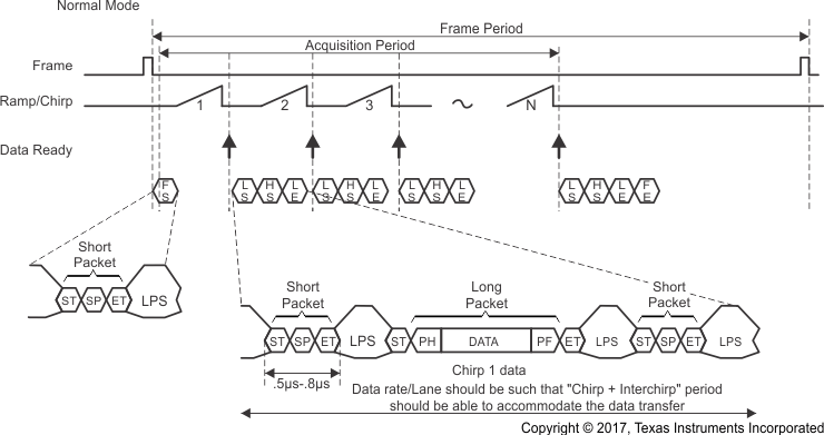
The AWR1243 device uses MIPI D-PHY / CSI2-based format to transfer the raw ADC samples to the external MCU. This is shown in Figure 9-5.
- Supports four data lanes
- CSI-2 data rate scalable from 150 Mbps to 600 Mbps per lane
- Virtual channel based
- CRC generation

Frame Start – CSi2 VSYNC Start Short PacketLine Start – CSI2 HSYNC Start Short PacketLine End – CSI2 HSYNC End Short PacketFrame End – CSi2 VSYNC End Short Packet
Figure 9-5 CSI-2 Transmission FormatThe data payload is constructed with the following three types of information:
- Chirp profile information
- The actual chirp number
- ADC data corresponding to chirps of all four
channels
- Interleaved fashion
- Chirp quality data (configurable)
The payload is then split across the four physical data lanes and transmitted to the receiving D-PHY. The data packet packing format is shown in Figure 9-6
 Figure 9-6 Data Packet Packing Format for 12-Bit Complex Configuration