SWRS194J January   2018  – November 2023 CC2642R

PRODUCTION DATA  

  1.   1
  2. Features
  3. Applications
  4. Description
  5. Functional Block Diagram
  6. Revision History
  7. Device Comparison
  8. Terminal Configuration and Functions
    1. 7.1 Pin Diagram – RGZ Package (Top View)
    2. 7.2 Signal Descriptions – RGZ Package
    3. 7.3 Connections for Unused Pins and Modules
  9. Specifications
    1. 8.1  Absolute Maximum Ratings
    2. 8.2  ESD Ratings
    3. 8.3  Recommended Operating Conditions
    4. 8.4  Power Supply and Modules
    5. 8.5  Power Consumption - Power Modes
    6. 8.6  Power Consumption - Radio Modes
    7. 8.7  Nonvolatile (Flash) Memory Characteristics
    8. 8.8  Thermal Resistance Characteristics
    9. 8.9  RF Frequency Bands
    10. 8.10 Bluetooth Low Energy - Receive (RX)
    11. 8.11 Bluetooth Low Energy - Transmit (TX)
    12. 8.12 Timing and Switching Characteristics
      1. 8.12.1 Reset Timing
      2. 8.12.2 Wakeup Timing
      3. 8.12.3 Clock Specifications
        1. 8.12.3.1 48 MHz Crystal Oscillator (XOSC_HF)
        2. 8.12.3.2 48 MHz RC Oscillator (RCOSC_HF)
        3. 8.12.3.3 2 MHz RC Oscillator (RCOSC_MF)
        4. 8.12.3.4 32.768 kHz Crystal Oscillator (XOSC_LF)
        5. 8.12.3.5 32 kHz RC Oscillator (RCOSC_LF)
      4. 8.12.4 Synchronous Serial Interface (SSI) Characteristics
        1. 8.12.4.1 Synchronous Serial Interface (SSI) Characteristics
        2.       35
      5. 8.12.5 UART
        1. 8.12.5.1 UART Characteristics
    13. 8.13 Peripheral Characteristics
      1. 8.13.1 ADC
        1. 8.13.1.1 Analog-to-Digital Converter (ADC) Characteristics
      2. 8.13.2 DAC
        1. 8.13.2.1 Digital-to-Analog Converter (DAC) Characteristics
      3. 8.13.3 Temperature and Battery Monitor
        1. 8.13.3.1 Temperature Sensor
        2. 8.13.3.2 Battery Monitor
      4. 8.13.4 Comparators
        1. 8.13.4.1 Low-Power Clocked Comparator
        2. 8.13.4.2 Continuous Time Comparator
      5. 8.13.5 Current Source
        1. 8.13.5.1 Programmable Current Source
      6. 8.13.6 GPIO
        1. 8.13.6.1 GPIO DC Characteristics
    14. 8.14 Typical Characteristics
      1. 8.14.1 MCU Current
      2. 8.14.2 RX Current
      3. 8.14.3 TX Current
      4. 8.14.4 RX Performance
      5. 8.14.5 TX Performance
      6. 8.14.6 ADC Performance
  10. Detailed Description
    1. 9.1  Overview
    2. 9.2  System CPU
    3. 9.3  Radio (RF Core)
      1. 9.3.1 Bluetooth 5.2 Low Energy
    4. 9.4  Memory
    5. 9.5  Sensor Controller
    6. 9.6  Cryptography
    7. 9.7  Timers
    8. 9.8  Serial Peripherals and I/O
    9. 9.9  Battery and Temperature Monitor
    10. 9.10 µDMA
    11. 9.11 Debug
    12. 9.12 Power Management
    13. 9.13 Clock Systems
    14. 9.14 Network Processor
  11. 10Application, Implementation, and Layout
    1. 10.1 Reference Designs
    2. 10.2 Junction Temperature Calculation
  12. 11Device and Documentation Support
    1. 11.1 Tools and Software
      1. 11.1.1 SimpleLink™ Microcontroller Platform
    2. 11.2 Documentation Support
    3. 11.3 Support Resources
    4. 11.4 Trademarks
    5. 11.5 Electrostatic Discharge Caution
    6. 11.6 Glossary
  13. 12Mechanical, Packaging, and Orderable Information
    1. 12.1 Packaging Information

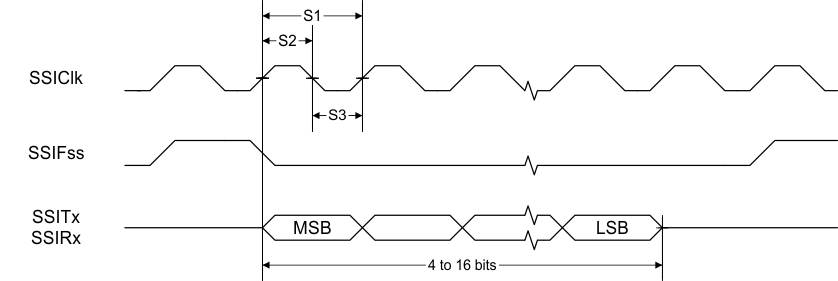
GUID-D126082D-D4D1-434F-9CE7-F3D445FAFCA8-low.gifFigure 8-1 SSI Timing for TI Frame Format (FRF = 01), Single Transfer Timing Measurement
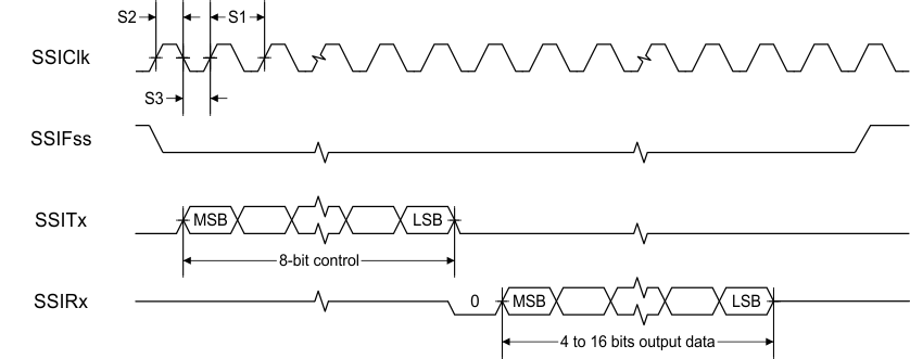
GUID-CC88115F-174C-44E5-A758-9D42CBDBBC71-low.gifFigure 8-2 SSI Timing for MICROWIRE Frame Format (FRF = 10), Single Transfer
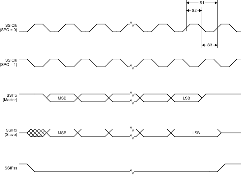
GUID-9AAED034-2567-4872-B08C-16032C0C62CC-low.gifFigure 8-3 SSI Timing for SPI Frame Format (FRF = 00), With SPH = 1