SWRS222D December 2018 – September 2024 AWR1843
PRODUCTION DATA
- 1
- 1 Features
- 2 Applications
- 3 Description
- 4 Functional Block Diagram
- 5 Device Comparison
- 6 Terminal Configuration and Functions
-
7 Specifications
- 7.1 Absolute Maximum Ratings
- 7.2 ESD Ratings
- 7.3 Power-On Hours (POH)
- 7.4 Recommended Operating Conditions
- 7.5 Power Supply Specifications
- 7.6 Power Consumption Summary
- 7.7 RF Specification
- 7.8 CPU Specifications
- 7.9 Thermal Resistance Characteristics for FCBGA Package [ABL0161]
- 7.10
Timing and Switching Characteristics
- 7.10.1 Power Supply Sequencing and Reset Timing
- 7.10.2 Input Clocks and Oscillators
- 7.10.3
Multibuffered / Standard Serial Peripheral Interface (MibSPI)
- 7.10.3.1 Peripheral Description
- 7.10.3.2
MibSPI Transmit and Receive RAM Organization
- 7.10.3.2.1 SPI Timing Conditions
- 7.10.3.2.2 SPI Controller Mode Switching Parameters (CLOCK PHASE = 0, SPICLK = output, SPISIMO = output, and SPISOMI = input) #GUID-C70CFB1F-161A-495B-85B8-62E1C643D037/T4362547-236 #GUID-C70CFB1F-161A-495B-85B8-62E1C643D037/T4362547-237 #GUID-C70CFB1F-161A-495B-85B8-62E1C643D037/T4362547-238
- 7.10.3.2.3 SPI Controller Mode Switching Parameters (CLOCK PHASE = 1, SPICLK = output, SPISIMO = output, and SPISOMI = input) #GUID-F724BCC6-8F26-42C4-8723-451EDE9A36D3/T4362547-244 #GUID-F724BCC6-8F26-42C4-8723-451EDE9A36D3/T4362547-245 #GUID-F724BCC6-8F26-42C4-8723-451EDE9A36D3/T4362547-246
- 7.10.3.3 SPI Peripheral Mode I/O Timings
- 7.10.3.4 Typical Interface Protocol Diagram (Peripheral Mode)
- 7.10.4 LVDS Interface Configuration
- 7.10.5 General-Purpose Input/Output
- 7.10.6 Controller Area Network Interface (DCAN)
- 7.10.7 Controller Area Network - Flexible Data-rate (CAN-FD)
- 7.10.8 Serial Communication Interface (SCI)
- 7.10.9 Inter-Integrated Circuit Interface (I2C)
- 7.10.10 Quad Serial Peripheral Interface (QSPI)
- 7.10.11 ETM Trace Interface
- 7.10.12 Data Modification Module (DMM)
- 7.10.13 JTAG Interface
- 8 Detailed Description
- 9 Monitoring and Diagnostics
- 10Applications, Implementation, and Layout
- 11Device and Documentation Support
- 12Revision History
- 13Mechanical, Packaging, and Orderable Information
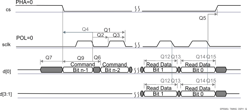
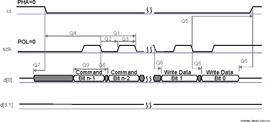
7.10.10.3 QSPI Switching Characteristics
| NO. | PARAMETER | MIN | TYP | MAX | UNIT | |
|---|---|---|---|---|---|---|
| Q1 | tc(SCLK) | Cycle time, sclk | 25 | ns | ||
| Q2 | tw(SCLKL) | Pulse duration, sclk low | 0.5*P – 3(1) | ns | ||
| Q3 | tw(SCLKH) | Pulse duration, sclk high | 0.5*P – 3 | ns | ||
| Q4 | td(CS-SCLK) | Delay time, sclk falling edge to cs active edge | –M*P – 1(2) | –M*P + 2.5(2) | ns | |
| Q5 | td(SCLK-CS) | Delay time, sclk falling edge to cs inactive edge | N*P – 1(2) | N*P + 2.5(2) | ns | |
| Q6 | td(SCLK-D1) | Delay time, sclk falling edge to d[0] transition | –3.5 | 7 | ns | |
| Q7 | tena(CS-D1LZ) | Enable time, cs active edge to d[0] driven (lo-z) | –P – 4(2) | –P +1(2) | ns | |
| Q8 | tdis(CS-D1Z) | Disable time, cs active edge to d[0] tri-stated (hi-z) | –P – 4(2) | –P +1(2) | ns | |
| Q9 | td(SCLK-D1) | Delay time, sclk first falling edge to first d[1] transition (for PHA = 0 only) | –3.5 – P(2) | 7 – P(2) | ns | |
(1) P = SCLK period in ns.
(2) M = QSPI_SPI_DC_REG.DDx + 1, N = 2
 Figure 7-14 QSPI Read (Clock Mode 0)
 Figure 7-15 QSPI Write (Clock Mode 0)