SWRS273D November 2021 – September 2024 AWR2944
PRODUCTION DATA
- 1
- 1 Features
- 2 Applications
- 3 Description
- 4 Device Comparison
- 5 Pin Configurations and Functions
-
6 Specifications
- 6.1 Absolute Maximum Ratings
- 6.2 ESD Ratings
- 6.3 Power-On Hours (POH)
- 6.4 Recommended Operating Conditions
- 6.5 VPP Specifications for One-Time Programmable (OTP) eFuses
- 6.6 Power Supply Specifications
- 6.7 Power Consumption Summary
- 6.8 RF Specifications
- 6.9 Thermal Resistance Characteristics
- 6.10 Power Supply Sequencing and Reset Timing
- 6.11 Input Clocks and Oscillators
- 6.12
Peripheral Information
- 6.12.1
QSPI Flash Memory Peripheral
- 6.12.1.1 QSPI Timing Conditions
- 6.12.1.2 QSPI Timing Requirements #GUID-CD30070D-F132-4A2C-92CD-5AA96AE70B94/GUID-97D19708-D87E-443B-9ADF-1760CFEF6F4C #GUID-CD30070D-F132-4A2C-92CD-5AA96AE70B94/GUID-0A61EEC9-2B95-4C27-B219-18D27C8F9430
- 6.12.1.3 QSPI Switching Characteristics #GUID-20B35D26-AFE6-451C-B9E9-B3F2FA08097C/T4362547-64 #GUID-20B35D26-AFE6-451C-B9E9-B3F2FA08097C/T4362547-65
- 6.12.2
Multibuffered / Standard Serial Peripheral Interface (MibSPI)
- 6.12.2.1 MibSPI Peripheral Description
- 6.12.2.2
MibSPI Transmit and Receive RAM Organization
- 6.12.2.2.1 SPI Timing Conditions
- 6.12.2.2.2 SPI Controller Mode Switching Parameters (CLOCK PHASE = 0, SPICLK = output, SPISIMO = output, and SPISOMI = input) #GUID-20BA2ACF-4FC2-43F6-960F-1A4CA56E65A6/T4362547-236 #GUID-20BA2ACF-4FC2-43F6-960F-1A4CA56E65A6/T4362547-237 #GUID-20BA2ACF-4FC2-43F6-960F-1A4CA56E65A6/T4362547-238
- 6.12.2.2.3 SPI Controller Mode Switching Parameters (CLOCK PHASE = 1, SPICLK = output, SPISIMO = output, and SPISOMI = input) #GUID-517E5284-3345-461F-B07F-EB95741B1272/T4362547-244 #GUID-517E5284-3345-461F-B07F-EB95741B1272/T4362547-245 #GUID-517E5284-3345-461F-B07F-EB95741B1272/T4362547-246
- 6.12.2.3 SPI Peripheral Mode I/O Timings
- 6.12.3
Ethernet Switch (RGMII/RMII/MII)
Peripheral
- 6.12.3.1 RGMII Timing Conditions
- 6.12.3.2 RGMII Transmit Clock Switching Characteristics
- 6.12.3.3 RGMII Transmit Data and Control Switching Characteristics
- 6.12.3.4 RGMII Receive Clock Timing Requirements
- 6.12.3.5 RGMII Receive Data and Control Timing Requirements
- 6.12.3.6 RMII Transmit Clock Switching Characteristics
- 6.12.3.7 RMII Transmit Data and Control Switching Characteristics
- 6.12.3.8 RMII Receive Clock Timing Requirements
- 6.12.3.9 RMII Receive Data and Control Timing Requirements
- 6.12.3.10 MII Transmit Switching Characteristics
- 6.12.3.11 MII Receive Clock Timing Requirements
- 6.12.3.12 MII Receive Timing Requirements
- 6.12.3.13 MII Transmit Clock Timing Requirements
- 6.12.3.14 MDIO Interface Timings
- 6.12.4 LVDS/Aurora Instrumentation and Measurement Peripheral
- 6.12.5 UART Peripheral
- 6.12.6 Inter-Integrated Circuit Interface (I2C)
- 6.12.7 Controller Area Network - Flexible Data-rate (CAN-FD)
- 6.12.8 CSI2 Receiver Peripheral
- 6.12.9 Enhanced Pulse-Width Modulator (ePWM)
- 6.12.10 General-Purpose Input/Output
- 6.12.1
QSPI Flash Memory Peripheral
- 6.13 Emulation and Debug
- 7 Detailed Description
- 8 Monitoring and Diagnostics
- 9 Applications, Implementation, and Layout
- 10Device and Documentation Support
- 11Revision History
- 12Mechanical, Packaging, and Orderable Information
6.12.8.1 CSI2 Switching Characteristics
over operating free-air temperature range (unless otherwise noted)
| PARAMETER | MIN | TYP | MAX | UNIT | |
|---|---|---|---|---|---|
| Low Power Receiver (LP-RX) | |||||
| VIL(1) | Logic 0 input threshold | 550 | mV | ||
| VIH(2) | Logic 1 input threshold | 880 | mV | ||
| VHYST | Input Hysteresis | 25 | mV | ||
| High Speed Receiver (HS-RX) | |||||
| VIDTH | Differential input high threshold | 70 | mV | ||
| VIDTL | Differential input low threshold | -70 | mV | ||
| VIDMAX | Maximum differential input voltage | 270 | mV | ||
| VILHS | Single-ended input low voltage | -40 | mV | ||
| VIHHS | Single-ended input high voltage | 460 | mV | ||
| VCMRXDC | Common-mode voltage | 70 | 330 | mV | |
| ΔVCMRX(HF) | Common-mode interference beyond 450 MHz | 200 | mVPP | ||
| ΔVCMRX(LF) | Common mode interference 50MHz – 450MHz | -50 | 50 | mVPP | |
| HS DATA-CLOCK Timing Specification(3)(5) | |||||
| UIINST | Data/Clock Unit Interval | 1.11 | ns | ||
| TSETUP | Data to Clock setup time | 166 | ps | ||
| THOLD | Clock to Data hold time | 166 | ps | ||
| TR, , TF(4) | Rise/Fall Times | 166 | 0.4*UIINST | ps | |
(1) The input low-level voltage, VIL, is the voltage at which the receiver is
required to detect a low state in the input signal. VIL is larger than the
maximum single-ended line voltage during HS transmission. Therefore, both LP
receivers will detect low during HS signaling
(2) The input high-level voltage, VIH, is the voltage at which the receiver is
required to detect a high state in the input signal.
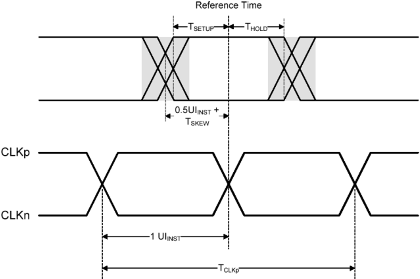
(3) TSKEW in the figure is the skew
between the clock and data HS signals that can be tolerated at the receiver
input. It is only a descriptive parameter. Rx timing is specified by
TSETUP/THOLD only.
(4) Rise/Fall from VIDTL to VIDTH.
(5) Setup/hold specification is assuming identical common mode and rise/fall time
for both data and clock lane at receiver input. i.e. VCMRXDC and
TR, TF must be same for clock lane and data lane while
measuring TSETUP and THOLD
 Figure 6-24 Clock and Data Timing in HS
Transmission