SWRU612 December 2023 CC3300 , CC3300MOD , CC3301 , CC3301MOD , CC3351 , CC3351MOD
- 1
- Abstract
- Trademarks
- 1Introduction
-
2Schematic Considerations
- 2.1 Schematic Reference Design
- 2.2 Power Supply
- 2.3 Clock Source
- 2.4 Radio Frequency (RF)
- 2.5 Digital Interfaces
- 3Layout Considerations
3.6 SDIO
SDIO is the main communication interface with the host processor for WLAN functions, and can also be used for BLE functions in shared SDIO protocols. These signals are especially sensitive because of the clock, and should be designed as such.
The SDIO lines include SDIO_CLK, SDIO_CMD, SDIO_D0, SDIO_D1, SDIO_D2, and SDIO_D3. The SDIO_CLK signal in particular is very sensitive and should be regarded as such. In order to ensure reliable SDIO communication, the following layout considerations should be taken into account:
- It is recommended that the SDIO lines have at least 5mils of width.
- The SDIO traces should be as far away as possible from the other digital or analog signal traces.
- It is recommended to add ground shielding around the SDIO bus.
- The SDIO_CLK must be isolated from all other signals with ground vias (stitching vias) and adjacent ground planes. The signal trace should have a clearance of at least twice the trace width of the other SDIO signals.
- Route the SDIO lines in parallel to each other with lengths as short as possible (to decrease propagation delay), and have a clearance of 1.5x the trace width.
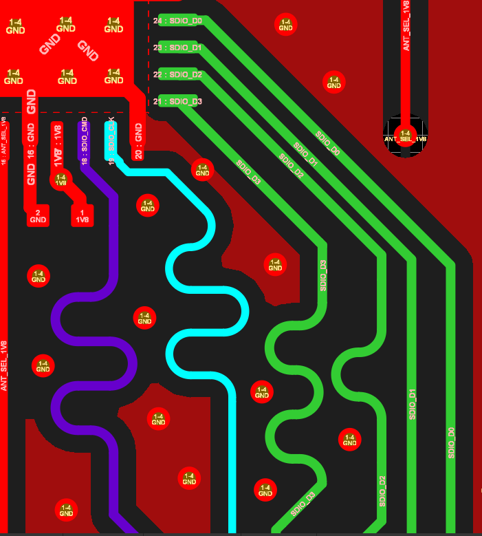
- The lengths of the SDIO traces must be length matched within 20 mil tolerance to provide the sampled data at the same time on all of the traces. For a visual example of length tuning, see Figure 3-15.
Figure 3-15 is sampled from the BP-CC3301 design files.
 Figure 3-15 Reference Layout for SDIO
Signals