SWRU612 December 2023 CC3300 , CC3301 , CC3351
- 1
- Abstract
- Trademarks
- 1Introduction
-
2Schematic Considerations
- 2.1 Schematic Reference Design
- 2.2 Power Supply
- 2.3 Clock Source
- 2.4 Radio Frequency (RF)
- 2.5 Digital Interfaces
- 3Layout Considerations
3.4 XTAL
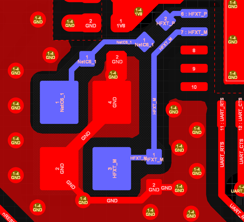
Figure 3-11 shows the placement and layout around the 40 MHz XTAL and its connections to the CC33xx IC.
Figure 3-11 is sampled from the BP-CC3301 design files.
 Figure 3-11 40MHz XTAL From
BP-CC3301
Figure 3-11 40MHz XTAL From
BP-CC3301When integrating the XTAL, please follow these guidelines:
- The traces connecting the XTAL to the CC3301 (XTAL_P and XTAL_M) be as short as possible with matching trace length.
- Place a 150 Ω resistor on the XTAL_P pin as close as possible to the CC33xx.
- The two loading capacitors should be parallel to the edge of the XTAL.
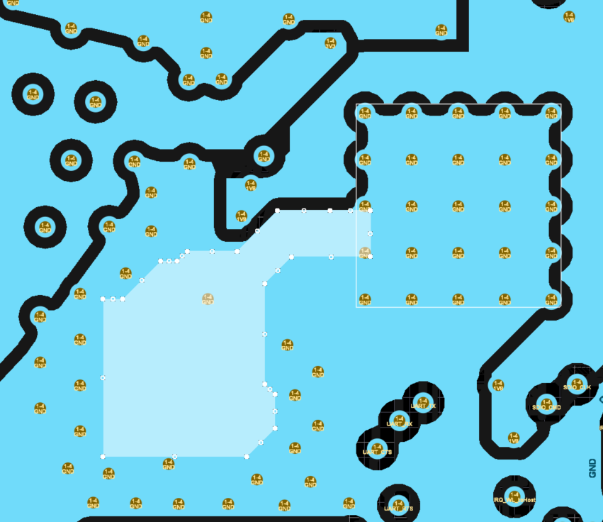
- On layer below the crystal (layer 2), place a cutout underneath the area of the XTAL and the loading capacitors. Check on the layer below that (layer 3) has good ground underneath the same area. For a visual representation, see Figure 3-12.
- Wherever possible, there should be increased ground via stitching around the XTAL for optimal isolation.
Figure 3-12 is sampled from layer 3 of the M2-CC3301 design files.
 Figure 3-12 Reference Layout for Layer
Under XTAL Cutout