SWRU613A July 2023 – August 2024 AWRL1432 , IWRL1432
- 1
- Description
- Get Started
- Features
- 5
- 1Evaluation Module Overview
-
2Hardware
- 2.1 XWRL1432BOOST Antenna
- 2.2 EVM Mux Block Diagram
- 2.3 Switch Settings
- 2.4 LEDs
- 2.5 Connectors
- 2.6 USB Connector
- 2.7 DCA1000 HD Connector
- 2.8 Booster Pack Connector for the LaunchPad Connectivity
- 2.9 CANFD Connector
- 2.10 LIN PHY Connection
- 2.11 I2C Connections
- 2.12 XDS110 Interface
- 2.13 Flashing the Board
- 2.14 DCA1000EVM Mode
- 2.15 PCB Storage and Handling Recommendations:
- 3Software
- 4Hardware Design Files
- 5Additional Information
- 6References
- 7Revision History
2.10 LIN PHY Connection
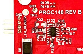
Figure 3-20 shows the LIN PHY (TLIN1039DDFRQ1) interface to the device. There are no switches for the LIN PHY interface. LIN PHY can operate with a different supply voltage than the mmWave sensor, an external VBAT option is provided for the LIN VDD supply, by default 5V_IN supply is provided.
 Figure 2-20 LIN header and PHY Interface
 Figure 2-21 LIN PHY Interface
To enable the external VBAT supply, resistor R32 needs to be mounted and resistor R31 needs to be removed.