SWRU613A July 2023 – August 2024 AWRL1432 , IWRL1432
- 1
- Description
- Get Started
- Features
- 5
- 1Evaluation Module Overview
-
2Hardware
- 2.1 XWRL1432BOOST Antenna
- 2.2 EVM Mux Block Diagram
- 2.3 Switch Settings
- 2.4 LEDs
- 2.5 Connectors
- 2.6 USB Connector
- 2.7 DCA1000 HD Connector
- 2.8 Booster Pack Connector for the LaunchPad Connectivity
- 2.9 CANFD Connector
- 2.10 LIN PHY Connection
- 2.11 I2C Connections
- 2.12 XDS110 Interface
- 2.13 Flashing the Board
- 2.14 DCA1000EVM Mode
- 2.15 PCB Storage and Handling Recommendations:
- 3Software
- 4Hardware Design Files
- 5Additional Information
- 6References
- 7Revision History
2.3 Switch Settings
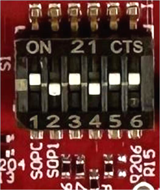
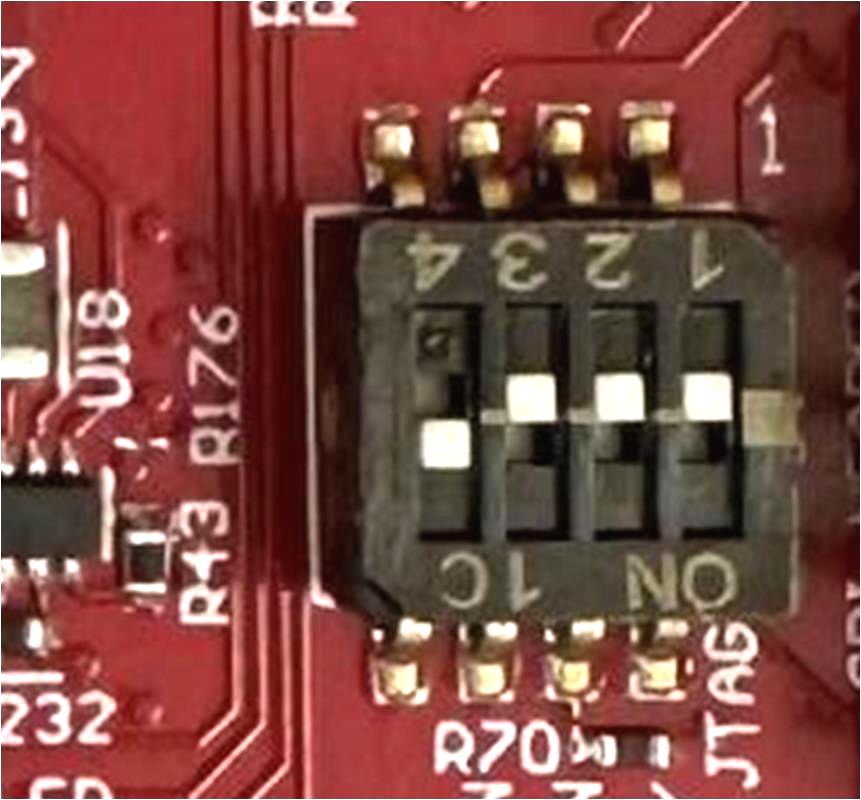
Figure 3-10 shows the part designators and positions of the switches (S1 and S4) on the XWRL1432BOOST.
 Figure 2-10 S1 Switch for Various Mode Settings
 Figure 2-11 S4 Switch for
Various Mode Settings
Figure 2-11 S4 Switch for
Various Mode SettingsFigure 3-12 shows the different boot mode configurations for the device. xWRL1432 supports Application mode/ Functional mode, Device management mode/ QSPI flashing mode, and Debug modes. The mode (SOP) configurations shown below in Figure 3-12 must be exercised first. After the correct SOP mode is set, an nRESET must be issued to register the SOP setting. Figure 3-13 provides the switch position settings for the Muxed signals functionality.
| SOP Mode | PMIC_CLK_OUT, TDO | Combination (S1.2, S1.1) |
| SOP_MODE1 | Device Management Mode/ QSPI Flashing Mode | 00 |
| SOP_MODE2 | Application mode/ Functional Mode | 01 |
| SOP_MODE4 | Debug Mode | 11 |
| Reference Designator | Switch ON | Switch OFF |
| S1.1 | SOP0 Pulled Up | SOP0 Pulled Down |
| S1.2 | SOP1 Pulled Up | SOP1 Pulled Down |
| S1.3 | LVDS | LIN_RX, XDS_UARTA/CAN, NERROR_LED, WATCH_DOG_TP, RTC_CLK_IN_TP, HOST_CLK_TP |
| S1.4 | XDS_RS232 | DCA_LP_RS232 |
| S1.5 | CAN | XDS_UARTA |
| S1.6 | I2C, REG_MODE, LED_SW_GPIO | SPI |
| S4.1 | XDS_JTAG | DCA_JTAG |
| S4.2 | CAN PHY: Stand by Mode Disable | CAN PHY: Stand by Mode Enable |
| S4.3 | LIN PHY: Enable | LIN PHY: Disable |
| S4.4 | - | - |