SWRU619A July 2024 – December 2024
- 1
- Description
- Applications
- Get Started
- Features
- 6
- 1Evaluation Module Overview
-
2Hardware
- 2.1 xWRL1432BOOST-BSD Antenna
- 2.2 EVM Mux Block Diagram
- 2.3 Switch Settings
- 2.4 LEDs
- 2.5 Connectors
- 2.6 USB Connector
- 2.7 DCA1000 HD Connector
- 2.8 Booster Pack Connector for the LaunchPad Connectivity
- 2.9 SPI-CAN Driver
- 2.10 CAN-FD Connector
- 2.11 LIN PHY Connection
- 2.12 I2C Connections
- 2.13 XDS110 Interface
- 2.14 Flashing the Board
- 2.15 DCA1000EVM Mode
- 2.16 PCB Storage and Handling Recommendations:
- 3Software
- 4Hardware Design Files
- 5Additional Information
- 6References
- Revision History
2.11 LIN PHY Connection
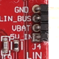
Figure 2-20 shows the LIN PHY (TLIN1039DDFRQ1) interface to the device. There are no switches for the LIN PHY interface. LIN PHY can operate with different supply voltage than the mmWave sensor, hence external VBAT option is provided for the LIN VDD supply, by default 5V_IN supply is provided. To enable external VBAT supply, R32 resistor need to be mounted and R31 resistor need to be removed.
 Figure 2-20 LIN header and PHY Interface
 Figure 2-21 LIN PHY Interface