SWRU619A July 2024 – December 2024
- 1
- Description
- Applications
- Get Started
- Features
- 6
- 1Evaluation Module Overview
-
2Hardware
- 2.1 xWRL1432BOOST-BSD Antenna
- 2.2 EVM Mux Block Diagram
- 2.3 Switch Settings
- 2.4 LEDs
- 2.5 Connectors
- 2.6 USB Connector
- 2.7 DCA1000 HD Connector
- 2.8 Booster Pack Connector for the LaunchPad Connectivity
- 2.9 SPI-CAN Driver
- 2.10 CAN-FD Connector
- 2.11 LIN PHY Connection
- 2.12 I2C Connections
- 2.13 XDS110 Interface
- 2.14 Flashing the Board
- 2.15 DCA1000EVM Mode
- 2.16 PCB Storage and Handling Recommendations:
- 3Software
- 4Hardware Design Files
- 5Additional Information
- 6References
- Revision History
2.1.1.1 Transmitter and Receiver Virtual Array
Transmitter and receiver antennas positions shown in Figure 2-6 form a virtual array of six transmitter-receiver pairs. This improves object detections by creating a finer azimuthal angular resolution (19°). Receiver antennas are spaced at distance D (Lambda/2) and Transmitter antenna Tx1 and Tx2 spaced at 1.5D (3lambda/2) in the azimuthal plane. No antenna elements are placed in the evilvational plane.
 Figure 2-6 Virtual Antenna Array
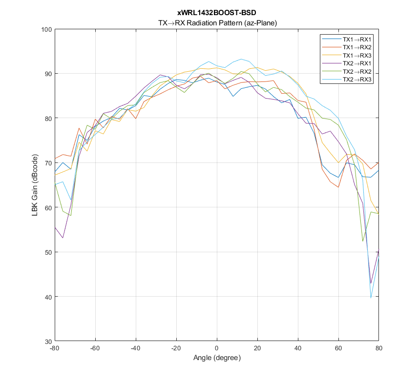
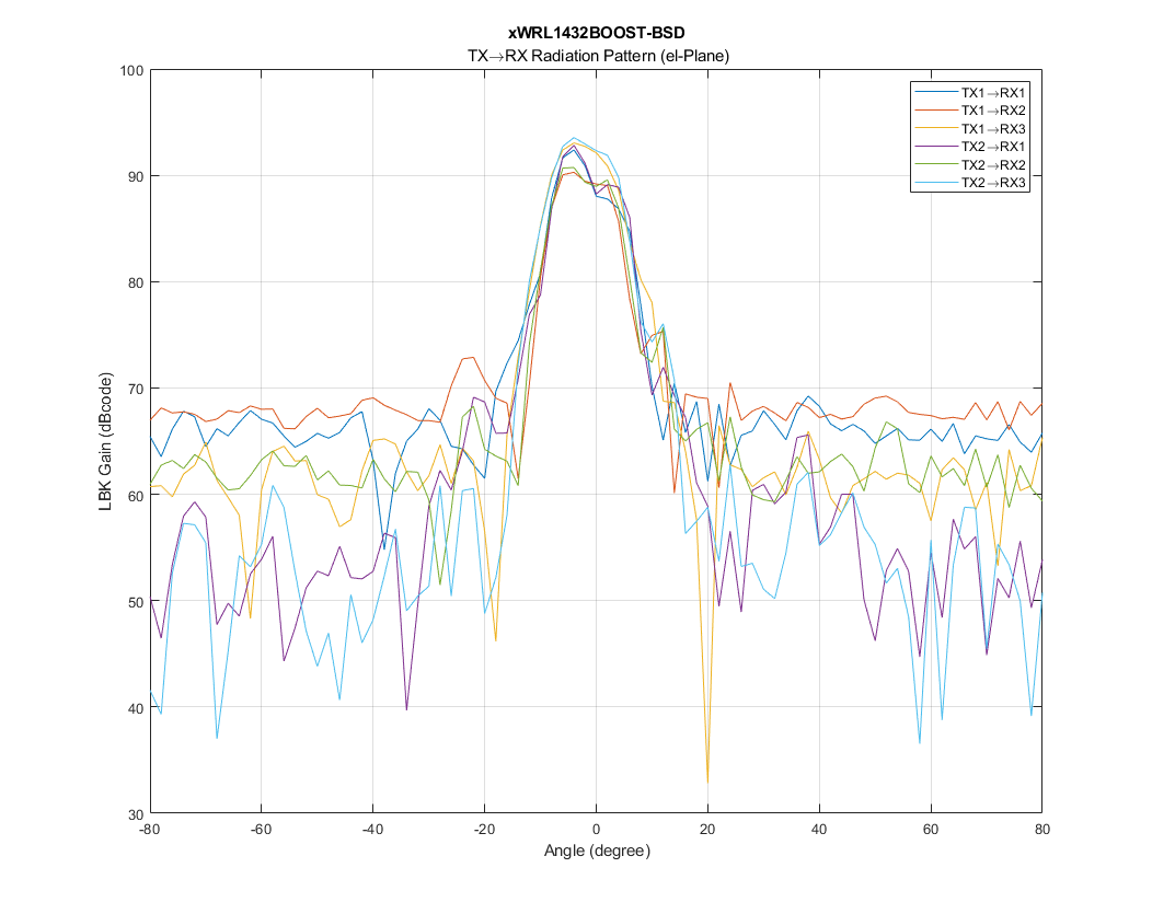
Figure 2-6 shows the antenna radiation pattern with regard to azimuth and the antenna radiation pattern with regard to elevation for TX1 and TX2. Both figures show the radiation pattern for TX1 and TX2 and RX1, RX2 and RX3 together. All of the measurements were done with a Tx and Rx combination together. Thus, for the -6dB beam width, the user must see a -12db (Tx (-6dB) + Rx(-6dB)) number from the boresight.
To reliably measure the complete virtual array radiation pattern in both the azithmal and elivational planes, a trihedral corner reflector was placed approximately 5 m from the EVM at boresight. The device was configured with a 1.0-GHz chirp and then swept across its azimuth and elevation. The raw ADC data was captured using a DCA-1000EVM and the resulting ADC data was post-processed. When visualized, it is possible to see the finer azithmal resolution in Figure 2-7 compared to lower elevational FoV seen in Figure 2-8.
 Figure 2-7 xWRL1432BOOST-BSD EVM Antenna Azithmal Radiation Pattern
 Figure 2-8 xWRL1432BOOST-BSD EVM Antenna Elevational Radiation Pattern