SWRU630 December 2024
- 1
- Description
- Getting Started
- Features
- 1Evaluation Module Overview
-
2Hardware
- 2.1 xWRL6844EVM Antenna
- 2.2 EVM Mux Block Diagram
- 2.3 Switch Settings
- 2.4 Push Button Switches
- 2.5 LEDs
- 2.6 DC Input Jack
- 2.7 USB Connector
- 2.8 DCA1000 HD Connector
- 2.9 BoosterPack Connector for LaunchPad Connectivity
- 2.10 CAN-FD_B Connector
- 2.11 CAN-FD_A Connector
- 2.12 LIN-PHY Connector
- 2.13 I2C Connections
- 2.14 XDS110 Interface
- 2.15 FTDI Interface
- 2.16 DCA1000EVM Mode
- 2.17 PCB Storage and Handling Recommendations:
- 3Software, Development Tools, and Example Code
- 4Hardware Design Files
- 5Additional Information
- 6References
- 7Revision History
2.3 Switch Settings
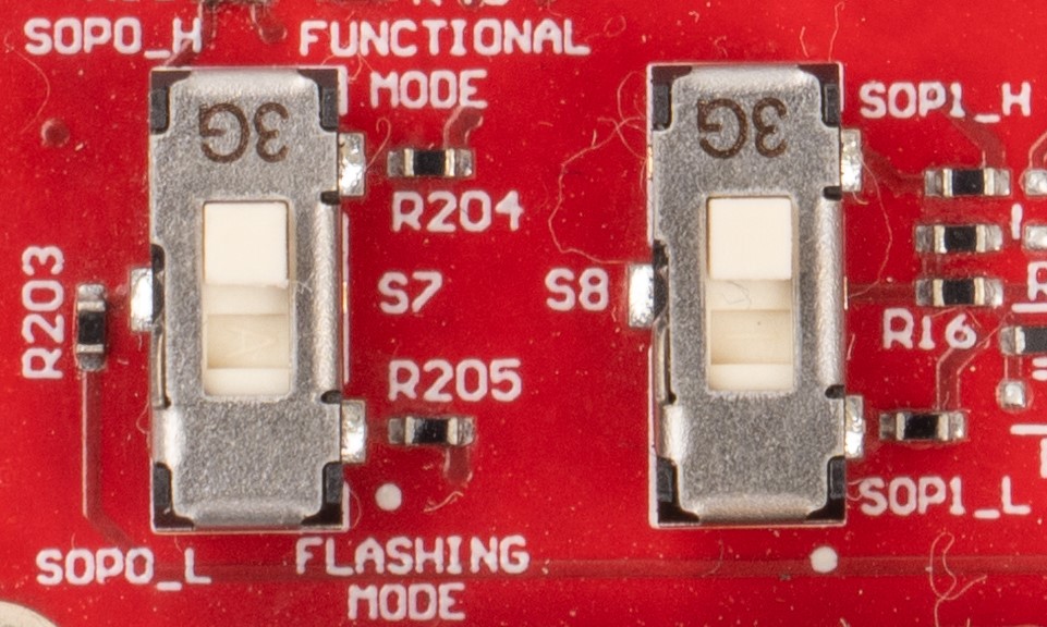
The Figure 2-10 shows the part designators and positions of the switches on xWRL6844EVM for different SOP mode settings. Table 2-1 shows the different boot mode configurations for the device. xWRL6844 supports Application mode/ Functional mode, Device management mode/ QSPI flashing mode, and Debug modes. The mode (SOP) configurations shown below Table 2-1 must be exercised first. After the correct SOP mode is set, an nRESET must be issued to register the SOP setting. In the Figure 2-10 the current SOP mode shown is Debug mode.
 Figure 2-10 SOP switches (S7, S8)
Table 2-1 SOP settings
| SOP Mode | PMIC_CLK_OUT, TDO | Combinations SOP1(S8), SOP0(S7) |
| SOP_MODE1 | Device Management Mode/ QSPI Flashing Mode | 00 |
| SOP_MODE2 | Application mode/ Functional Mode | 01 |
| SOP_MODE4 | Debug Mode/ Development Mode | 11 |
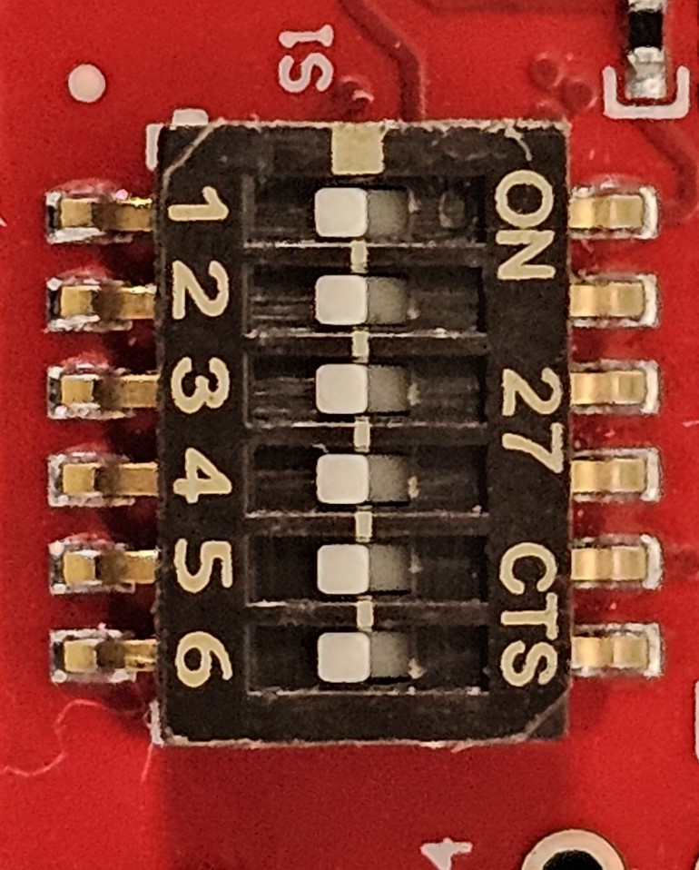
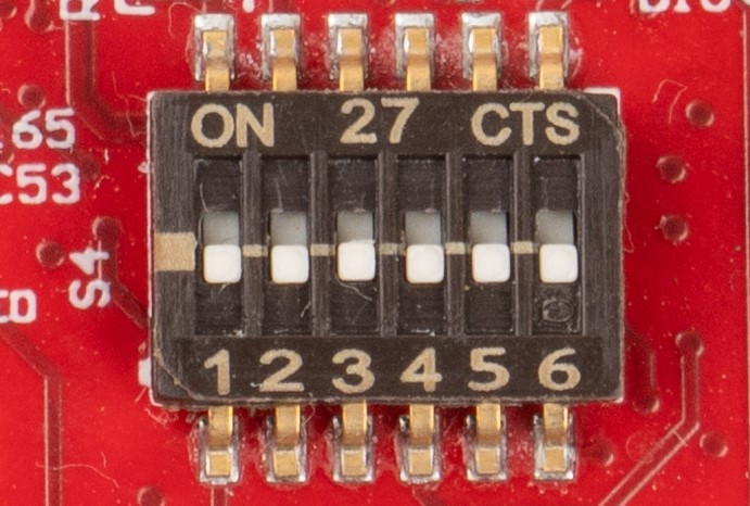
The S1 and S4 slide switches allows user connect to the digital interfaces from different peripherals
 Figure 2-11 Slide Switch (S1)
Table 2-2 S1 Switch Settings
| Reference Designator | Switch OFF | Switch ON |
|---|---|---|
| S1.1 | CAN PHY B: Stand by Mode Disable | CAN PHY B: Stand by Mode Enable |
| S1.2 | XDS_RS232 | FTDI_DCA_LP/BP_RS232 |
| S1.3 | FTDI_RS232 | DCA_LP/BP_RS232 |
| S1.4 | CAN_FD_A | XDS_DCA_LP/BP_FTDI_UARTA |
| S1.5 | DCA_LP/BP_FTDI_UARTA | XDS_UARTA |
| S1.6 | FTDI_UARTA | DCA_LP/BP_UARTA |
 Figure 2-12 Slide Switch (S4)
Table 2-3 S4 Switch Settings
| Reference Designator | Switch OFF | Switch ON |
|---|---|---|
| S4.1 | CAN PHY A: Stand by Mode Disable | CAN PHY A: Stand by Mode Enable |
| S4.2 | LIN PHY: Enable | LIN PHY: Disable |
| S4.3 | FTDI_SPI | DCA_SPI |
| S4.4 | XDS_JTAG | DCA_JTAG |
| S4.5 | UARTB | LIN |
| S4.6 | SPIB | I2C/HOST_CLK_REQ/SYS_RST_OUT |