SWRU631 November 2024
- 1
- Description
- Get Started
- Features
- 5
- 1Evaluation Module Overview
-
2Hardware
- 2.1 PCB Handling Recommendations
- 2.2 Power Connections
- 2.3 Connectors
- 2.4 Antenna
- 2.5 PMIC
- 2.6 On-Board Sensors
- 2.7 PC Connection
- 2.8 Connecting the AWR2E44PEVM to the DCA1000 EVM
- 2.9 Jumpers, Switches, and LEDs
- 3Software
- 4Hardware Design Files
- 5Additional Information
- 6Revision History
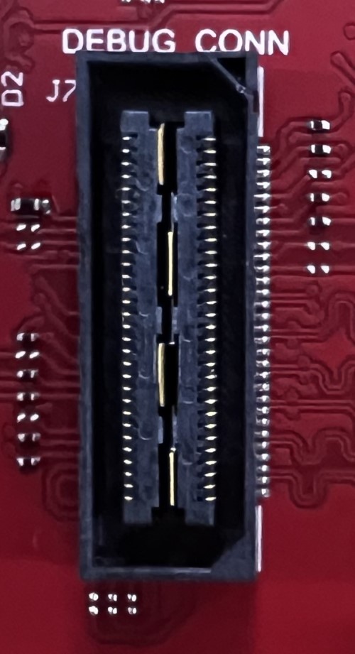
2.3.2 Debug Connector-60 pin (J7)
This connector enables interfacing of LVDS signals to the DCA1000 EVM for data capturing purposes.
Also, the connector has SPI, I2C, JTAG, GPADC, WRMRST, NRROUT, EPWM, and other control signals from AWR2E44PEVM for debug purpose.
The SPI is multiplexed to the Debug Connector. For more details refer to Section 2.7.1.
The debug connector supports direct connection to the TMDS273GPEVM for CSI2 data processing. For more details refer to CSI2 FE Connector ECO List.
 Figure 2-5 60-pin Debug Connector
Table 2-2 provides the pin assignment details for the Debug 60-pin connector.
Table 2-2 J7 Pin Assignment
| Pin Number | Description | Pin Number | Description |
|---|---|---|---|
| 1 | NC | 2 | NC |
| 3 | NC | 4 | XREF_CLK0 |
| 5 | GND | 6 | MSS_EPWMA0 |
| 7 | DBG_SPI_CS0 | 8 | GND |
| 9 | DBG_SPI_CLK | 10 | MSS_SPIA_HOSTIRQ |
| 11 | DBG_SPI_PICO | 12 | DBG_SPI_POCI |
| 13 | 3.3V PULL_UP | 14 | XREF_CLK1 |
| 15 | EMU_TCK | 16 | AR_SYNCIN |
| 17 | EMU_TDI | 18 | GND |
| 19 | GPADC1 | 20 | EMU_TMS |
| 21 | GPADC2 | 22 | EMU_TDO |
| 23 | NC | 24 | GND |
| 25 | NC | 26 | CSI2_TX2_CLK_LVDS_FRCLK_P |
| 27 | GPADC5 | 28 | CSI2_TX2_CLK_LVDS_FRCLK_N |
| 29 | GPADC6 | 30 | GND |
| 31 | NC | 32 | CSI2_TX3_P |
| 33 | MCU_CLKOUT | 34 | CSI2_TX3_N |
| 35 | NC | 36 | GND |
| 37 | MSS_SPIB_CS1 | 38 | CSI2_TX2_CLK_LVDS_FRCLK_P |
| 39 | SOP1_MSS_SPIB_CS2 | 40 | CSI2_TX2_CLK_LVDS_FRCLK_N |
| 41 | MSS_GPIO_0 | 42 | GND |
| 43 | MSS_GPIO_1 | 44 | CSI2_TX4_LVDS_CLK_P |
| 45 | AR_WRMRST | 46 | CSI2_TX4_LVDS_CLK_N |
| 47 | NC | 48 | GND |
| 49 | AR_NERROUT | 50 | CSI2_TX1_LVDS_TX1_P |
| 51 | MSS_I2CA_SCL | 52 | CSI2_TX1_LVDS_TX1_N |
| 53 | MSS_I2CA_SDA | 54 | |
| 55 | MSS_EPWMB0 | 56 | CSI2_TX0_LVDS_TX0_P |
| 57 | MSS_EPWMA1 | 58 | CSI2_TX0_LVDS_TX0_N |
| 59 | MSS_GPIO_3 | 60 | GND |