TIDT012 February 2022
3.1 Switching
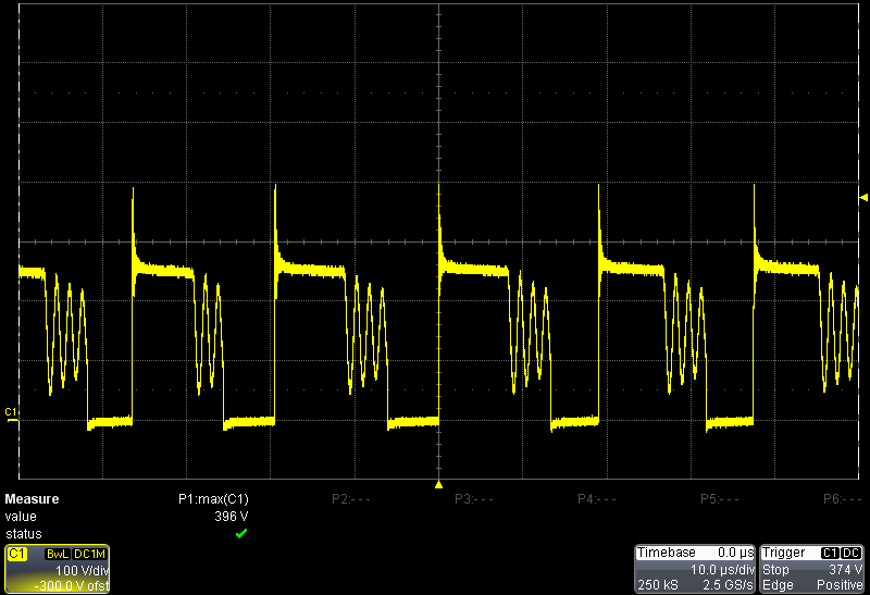
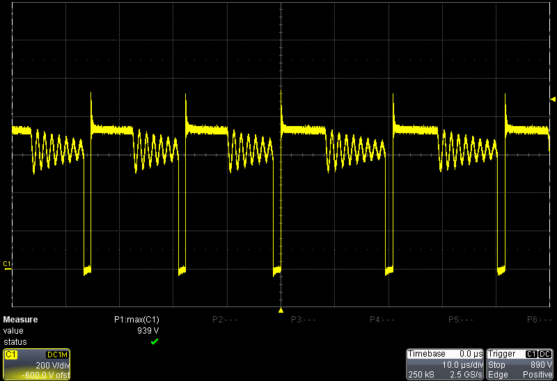
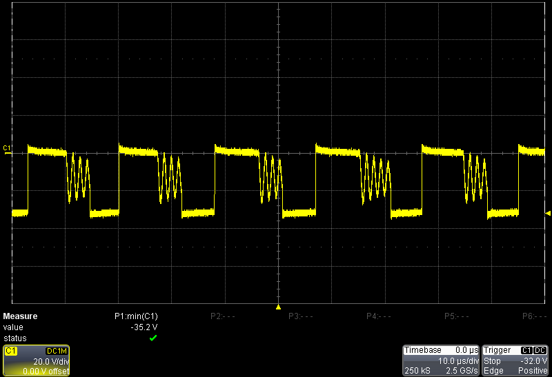
Figure 3-1 through Figure 3-3 illustrate the switching behavior. The switch node was measured with both outputs at full load.
 Figure 3-1 Primary Switching Node With 120-VAC
Input
 Figure 3-2 Primary Switching Node With 600-VDC
Input
 Figure 3-3 Secondary Switching Node With
120-VAC Input