TIDT193 August 2020 – MONTH
3.6 Input Voltage Transient Response
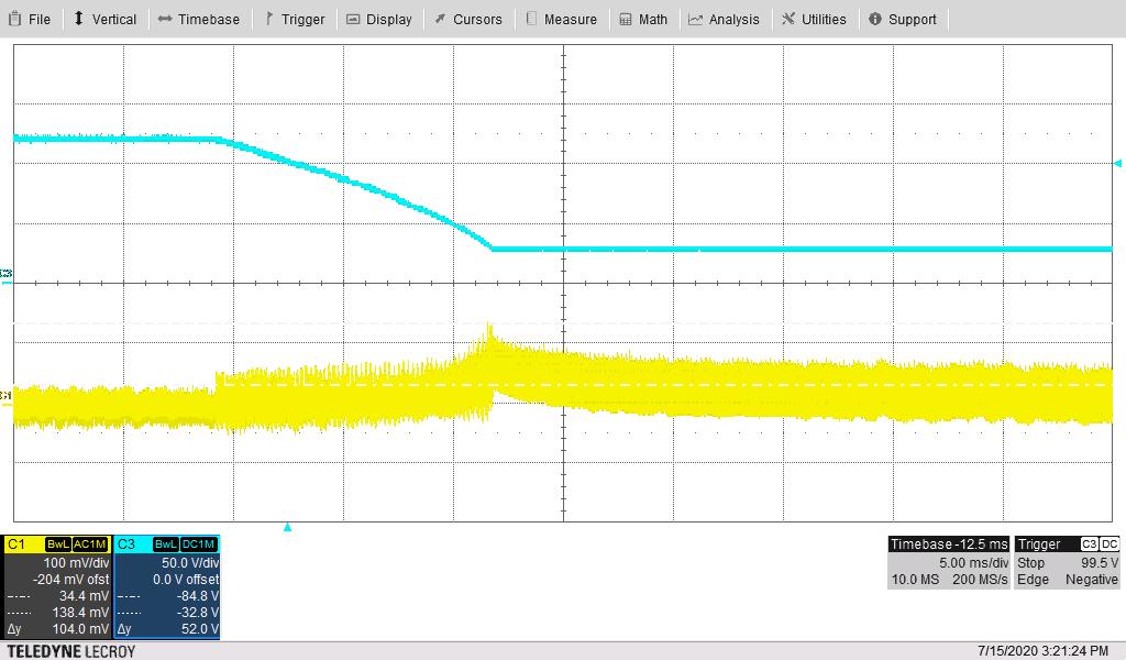
The following image shows the 14-V output voltage (AC coupled) (YELLOW) when the input voltage transitions from 120 V to 30 V (BLUE), 14 V is loaded to 130 mA.
 Figure 3-25 Input Voltage Transient Response (VOUT: 100 mV/div, VIN: 200 mA/div, 50 ms/div)
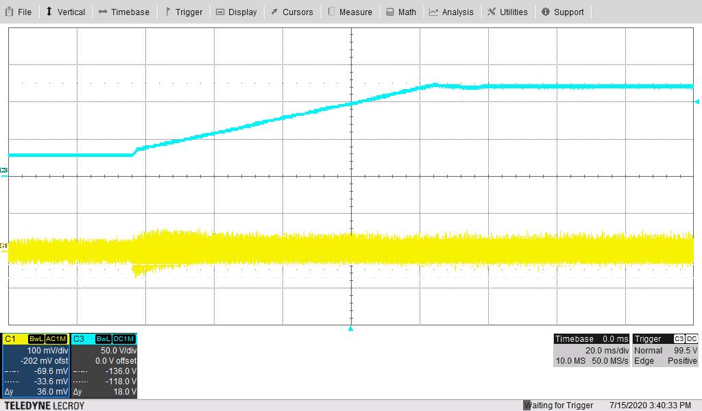
The following image shows the 14-V output voltage (AC coupled) (YELLOW) when the input voltage transitions from 30 V to 120 V (BLUE), 14 V is loaded to 130 mA.
 Figure 3-26 Input Voltage Transient Response (VOUT: 5 V/div, IOUT: 200 mA/div, 50 ms/div)