TIDT199A January 2021 – December 2022
2.1 Efficiency Graphs
The following graphs were measured at buck output (VOUT_A).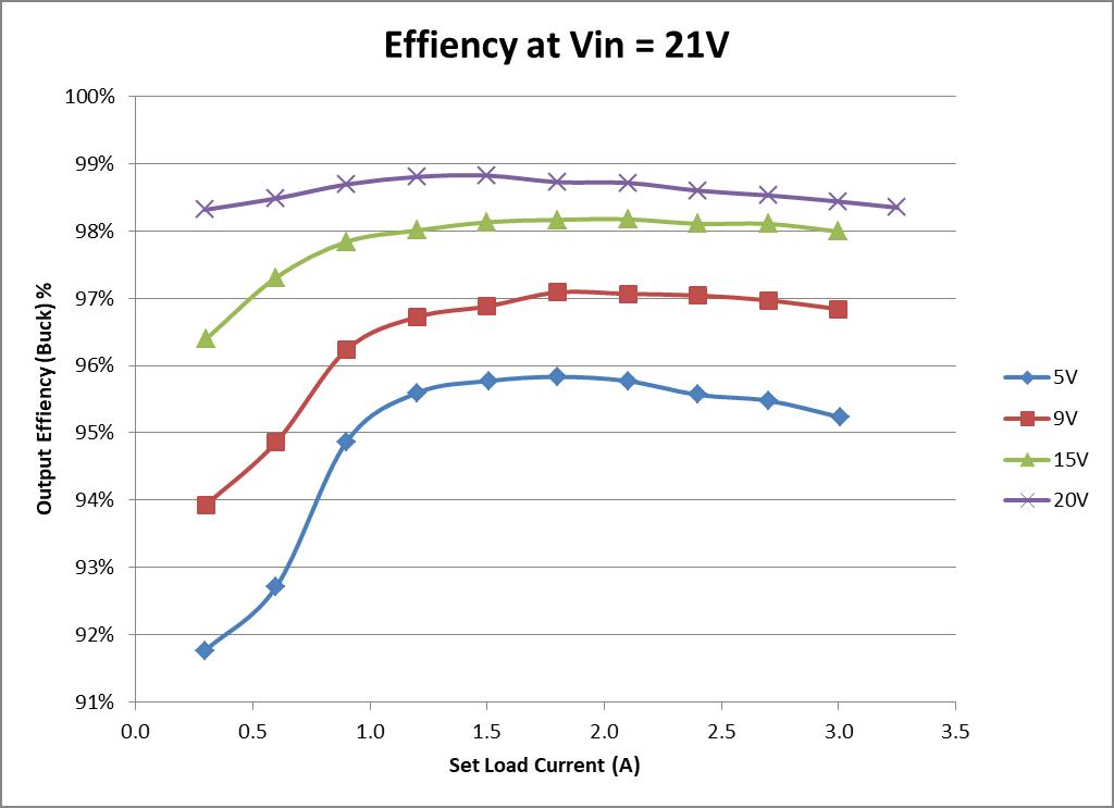 Figure 2-1 Efficiency by Output Voltage
 Figure 2-1 Efficiency by Output Voltage
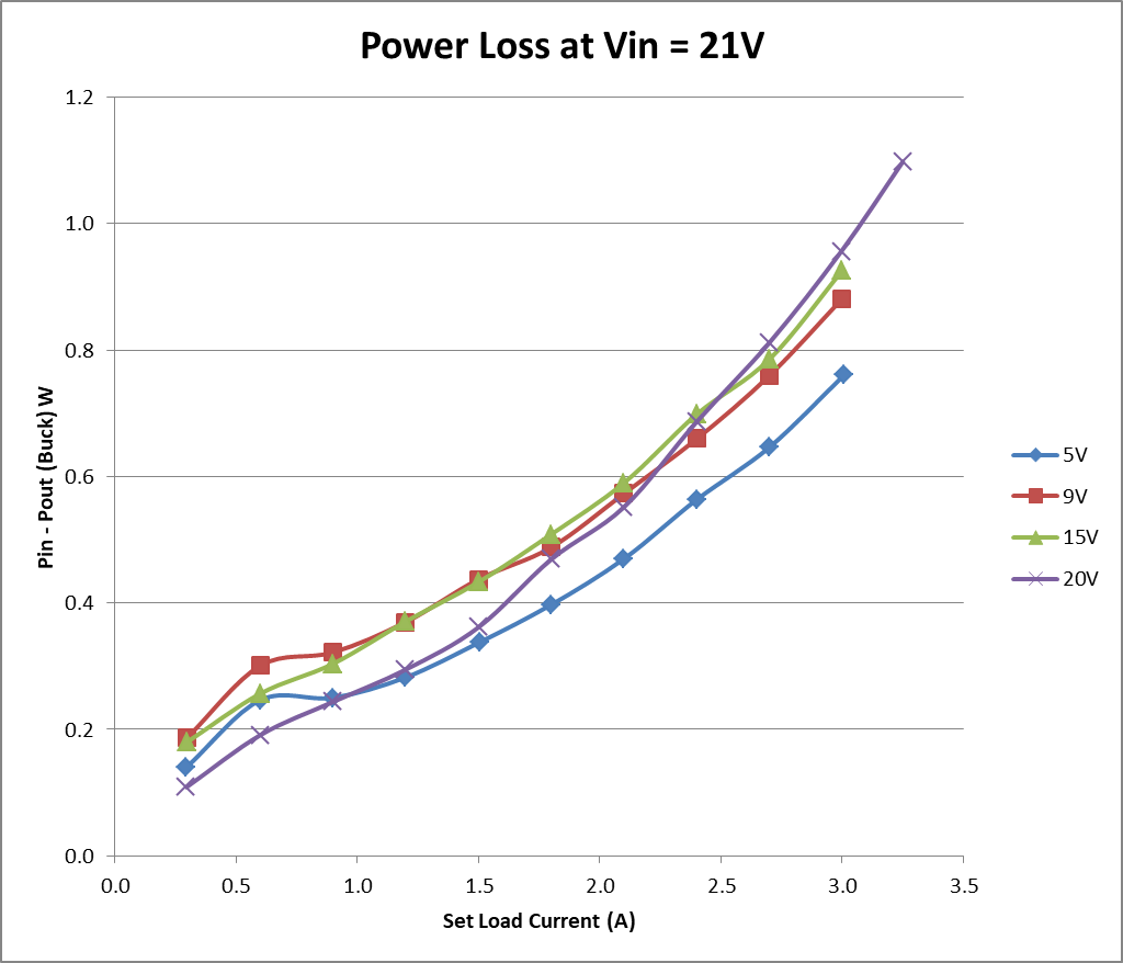 Figure 2-2 Loss by Output Voltage
TIDT199A January 2021 – December 2022
 Figure 2-1 Efficiency by Output Voltage
 Figure 2-2 Loss by Output Voltage