TIDT222 April   2021


  1. 1Description
  2. 2Test Prerequisites
    1. 2.1 Voltage and Current Requirements
    2. 2.2 Required Equipment
    3. 2.3 Considerations
    4. 2.4 Dimensions
    5. 2.5 Test Setup
  3. 3Testing and Results
    1. 3.1 Efficiency and Loss Graphs
    2. 3.2 Efficiency Data
    3. 3.3 Thermal Images
    4. 3.4 Bode Plots
  4. 4Waveforms
    1. 4.1 Switching
    2. 4.2 Output Voltage Ripple
    3. 4.3 Load Transients
    4. 4.4 Start-up Sequence

Load Transients

Figure 4-7 shows the 1.2-V output voltage when the load current is stepped between 125 A and 200 A. An external static load of 125 A was used along with onboard dynamic load for 75-A pulses. The other parameters follow:

  • VIN = 12 V, rise 11.85 A/μs, fall 12.5 A/μs (10 mV/DIV, 10 A/DIV, 200 μs/DIV)

The dynamic load response measured at VOUT is measured on the bottom side of the board using a coaxial connection: see Test Setup.

The measured maximum overshoot of 20.4 mV above nominal 1 V or 2.04% above nominal. The measured maximum undershoot of 23.9 mV below nominal 1 V or 2.39% below nominal.

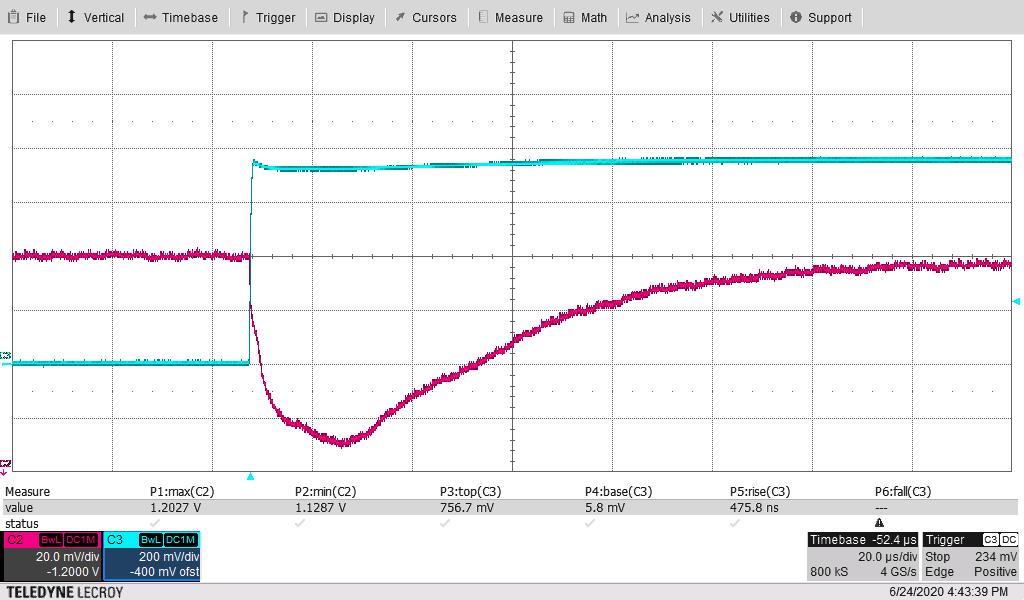
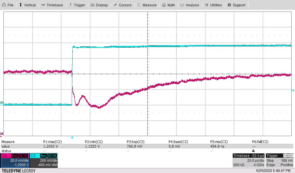
  • The current-sense waveform below is across a 10-mΩ resistor to ground on the dynamic load.
  • Blue trace J500 on board

Hence, the “top” of this pulse of 750 mV above the base divided by 10 mΩ, corresponds to a 75-A pulse.

  • dI/dT of rise is 80% of this 75 A (as rise time is defined for “10% to 90%” or 80%”) or 60 A divided by the rise time of 481 ns; or 60/0.48 or 125 A/μs. Rise time readings were 454–481 ns, 481 ns is used to estimate the dI/dT.
  • dI/dT of fall is 80% of this 20 A (as fall time is defined for “90% to 10%” or 80%”) or 60 A divided by the fall time of 360 ns; or 60/0.36 or –165 A/μs. Fall time readings were 340 ns–360 ns, 360 ns is used to estimate the dI/dT.
GUID-20210105-CA0I-QFZ5-DNNH-V9RBHKWG6Z2Q-low.jpg
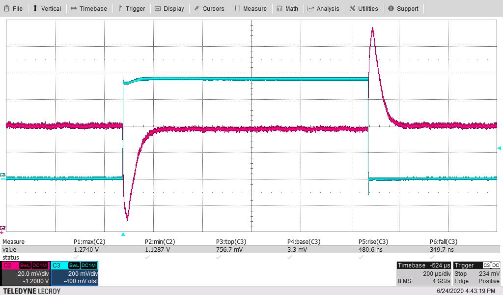
Looking at both load step of 75 A from 125 A to 200 A, and load dump back to 125 A
Red trace being VOUT on J501, blue trace dynamic I across 10 mΩ
Pinstrap set loop of 23-kHz crossover: minimum VOUT at 71 mV below 1.2 V and max at 74 mV above 1.2 V
Figure 4-7 Load Step, Dump 125 A-200 A-125 A, 23-kHz Crossover
GUID-20210105-CA0I-RGM7-Q6MK-T8CQKSKVPQML-low.jpg
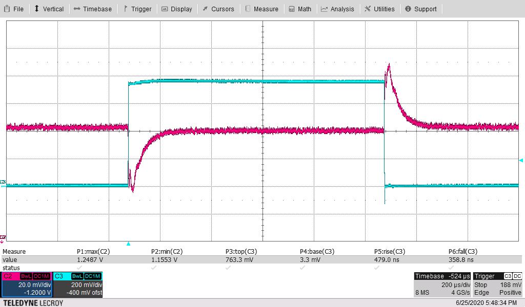
NVM loop Code11408458C2 for 36-kHz crossover: minimum VOUT at 45 mV below 1.2 V and max at 49 mV above 1.2 V
Figure 4-8 Load Step, Dump 125 A-200 A-125 A, 36-kHz Crossover

Figure 4-9 through Figure 4-12 are the same pair of waveforms, adjusting the time scale to highlight the load step and load-dump responses.
GUID-20210105-CA0I-DDP4-C6DP-LK7JRCSSSM6N-low.jpg
Focusing on load step of 75 A from 125 A to 200 A
Red trace being VOUT on J501, blue trace J500 dynamic I across 10 mΩ (75-A step at 125 A/μs)
Pinstrap set loop of 23-kHz crossover: minimum VOUT at 71 mV below 1.2 V
Figure 4-9 125 A–200 A Load Step, 23-kHz Crossover
GUID-20210105-CA0I-DLF8-9HVV-9QL1DXSHQHMQ-low.jpg
NVM loop Code11408458C2 for 36-kHz crossover: minimum VOUT at 45 mV below 1.2 V
Figure 4-10 125 A–200 A Load Step, 36-kHz Crossover
GUID-20210105-CA0I-ZLW5-LX2X-MZ0NKLLJ599T-low.jpg
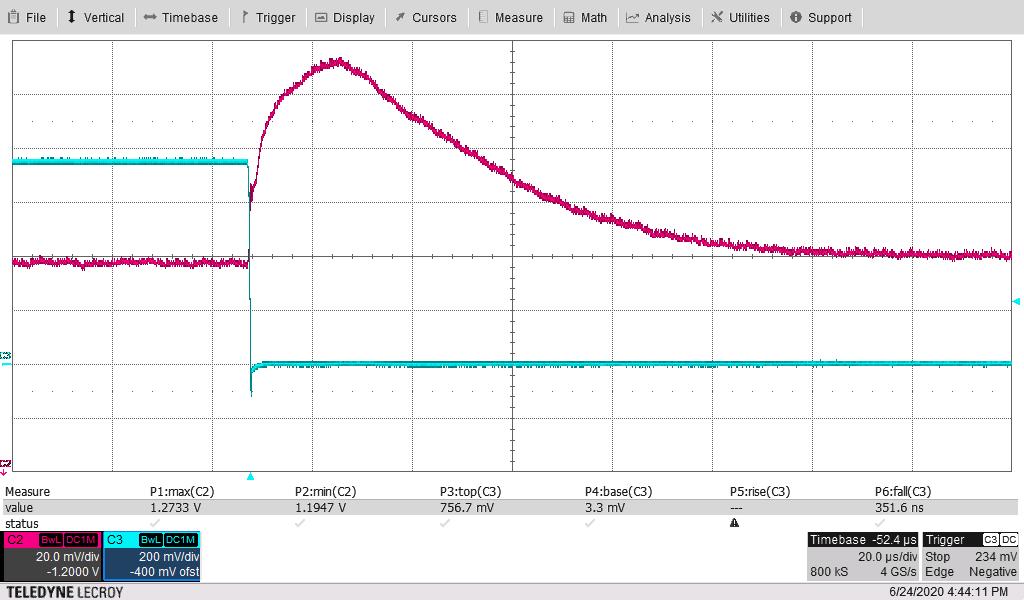
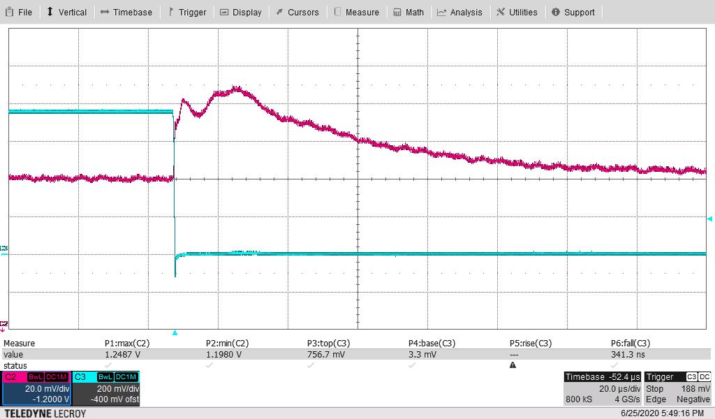
Focusing on load dump from 200 A back to 125 A.
Red trace being VOUT on J501, blue trace J500 dynamic I across 10 mΩ for 75A dump at –165 A/μs
Pinstrap set loop of 23-kHz crossover: max at 73 mV above 1.2 V
Figure 4-11 125 A–200 A Load Dump, 23-kHz Crossover
GUID-20210105-CA0I-TKBC-MWHF-Q0XXZ4Z6H0LS-low.jpg
NVM loop code11408458C2 for 36-kHz crossover: maximum at 49 mV above 1.2 V
Figure 4-12 125 A–200 A Load Dump, 36-kHz Crossover