TIDT222 April 2021
3.4 Bode Plots
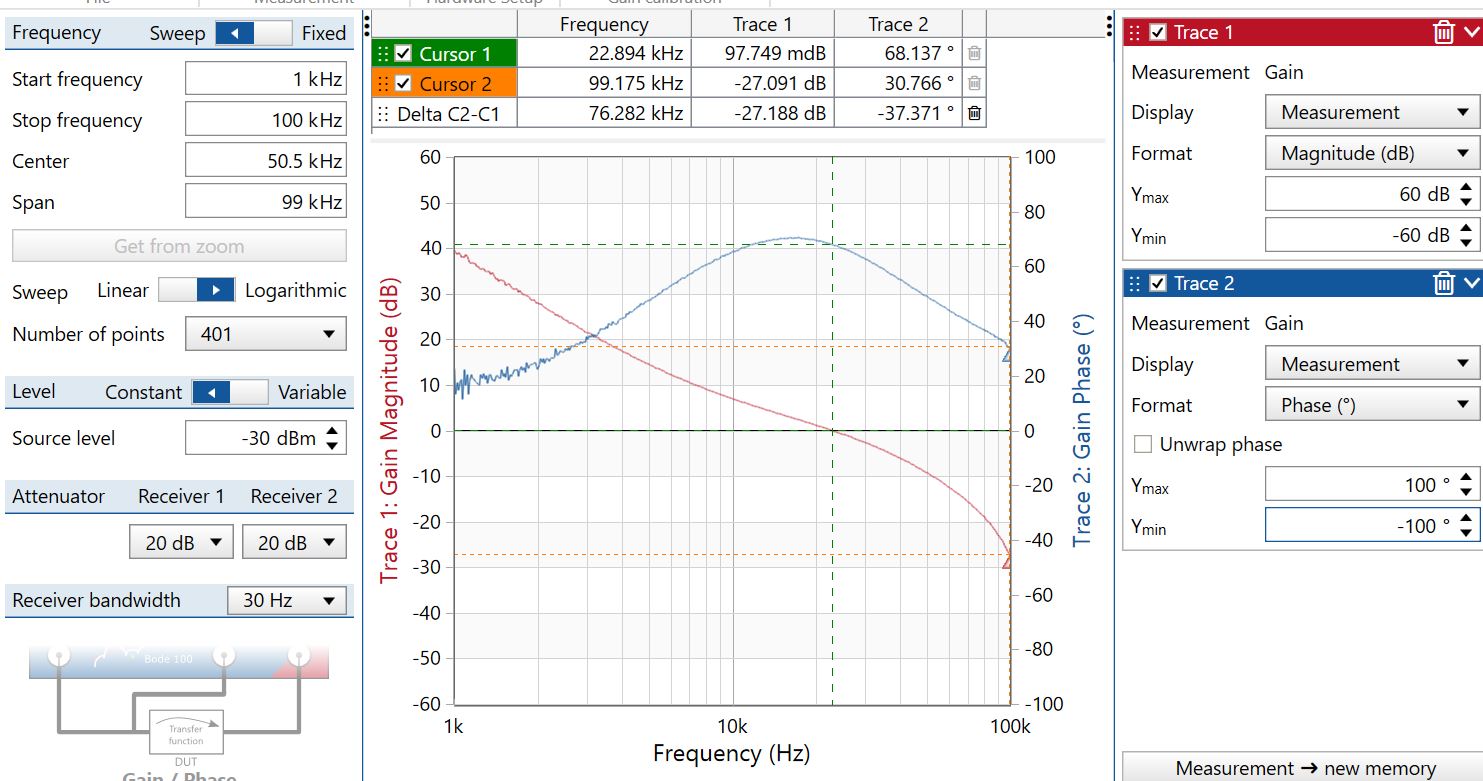
The following plot shows the loop gain and phase margin of the converter when loaded to 1.2 V at 40 A.
- VIN = 12 V, Bandwidth = 23 kHz , Phase Margin = 68 degrees
The loop is set by pinstrap resistors using 550 kHz and compensation code 18 as the fastest loop allowed among the 32 pinstrap selections:
 Figure 3-7 Bode Plot, Pinstrap Resistors
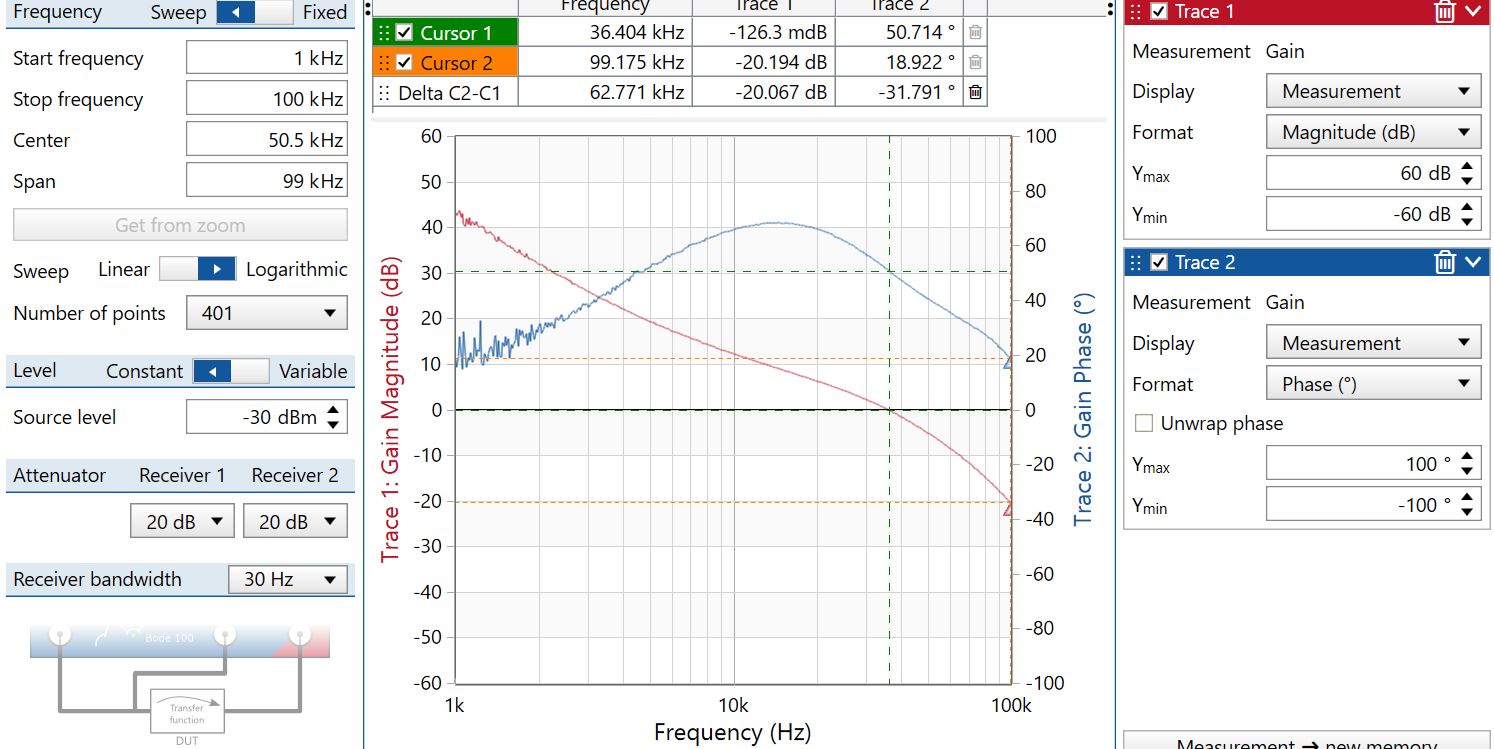
Loop set up using Nonvolatile Memory (NVM) programming which allows for many more than 32 compensation selections.
- Code11408458C2 used: 36-kHz bandwidth and 51 degrees of phase margin
 Figure 3-8 Bode Plot, NVM