TIDT222 April 2021
4.2 Output Voltage Ripple
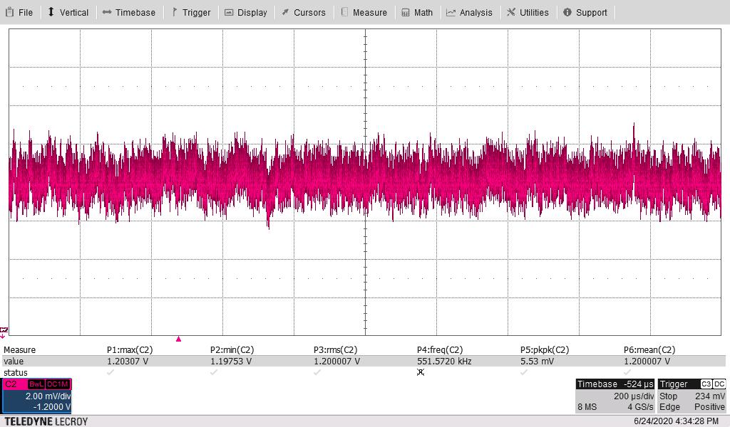
The output ripple voltage is shown in the following figures. The images were taken with the 1.2-V output loaded to 160 A and the input voltage set to 12 V.
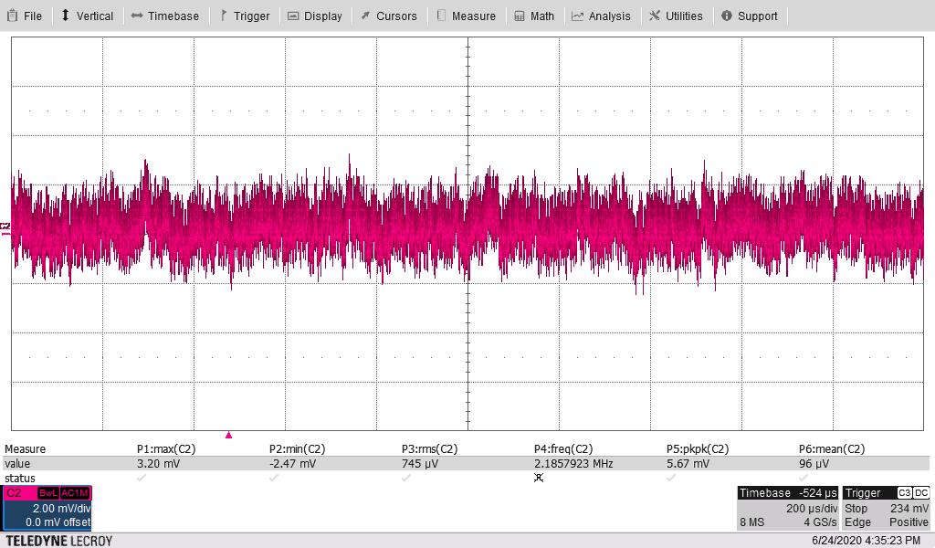
Both voltage ripple scopes were taken at 2 mV/DIV, 200 μs/DIV, 20-MHz bandwidth with onboard Vsense J501 and 1x probe. Ripple measurement was taken using connections on the bottom side of the board. Peak-to-peak ripple is 5.5 mV.
RMS of this ripple is based upon the same waveform and AC coupling was 745 μV.
 Figure 4-5 Output Voltage Ripple
  Figure 4-6 Output Voltage Ripple RMS, AC Coupling