TIDT224 March   2021


  1. 1Description
  2. 2Test Prerequisites
    1. 2.1 Voltage and Current Requirements
    2. 2.2 Required Equipment
  3. 3Testing and Results
    1. 3.1 Thermal Images
    2. 3.2 Efficiency and Power Dissipation Graphs
    3. 3.3 Efficiency and Power Dissipation Data
    4. 3.4 Voltage Regulation Graphs
    5. 3.5 Cross-Load Voltage Regulation Data and Efficiency
  4. 4Waveforms
    1. 4.1 Start-up Sequence
    2. 4.2 Switch Node
    3. 4.3 Output Voltage Ripple
    4. 4.4 Load Transients

Thermal Images

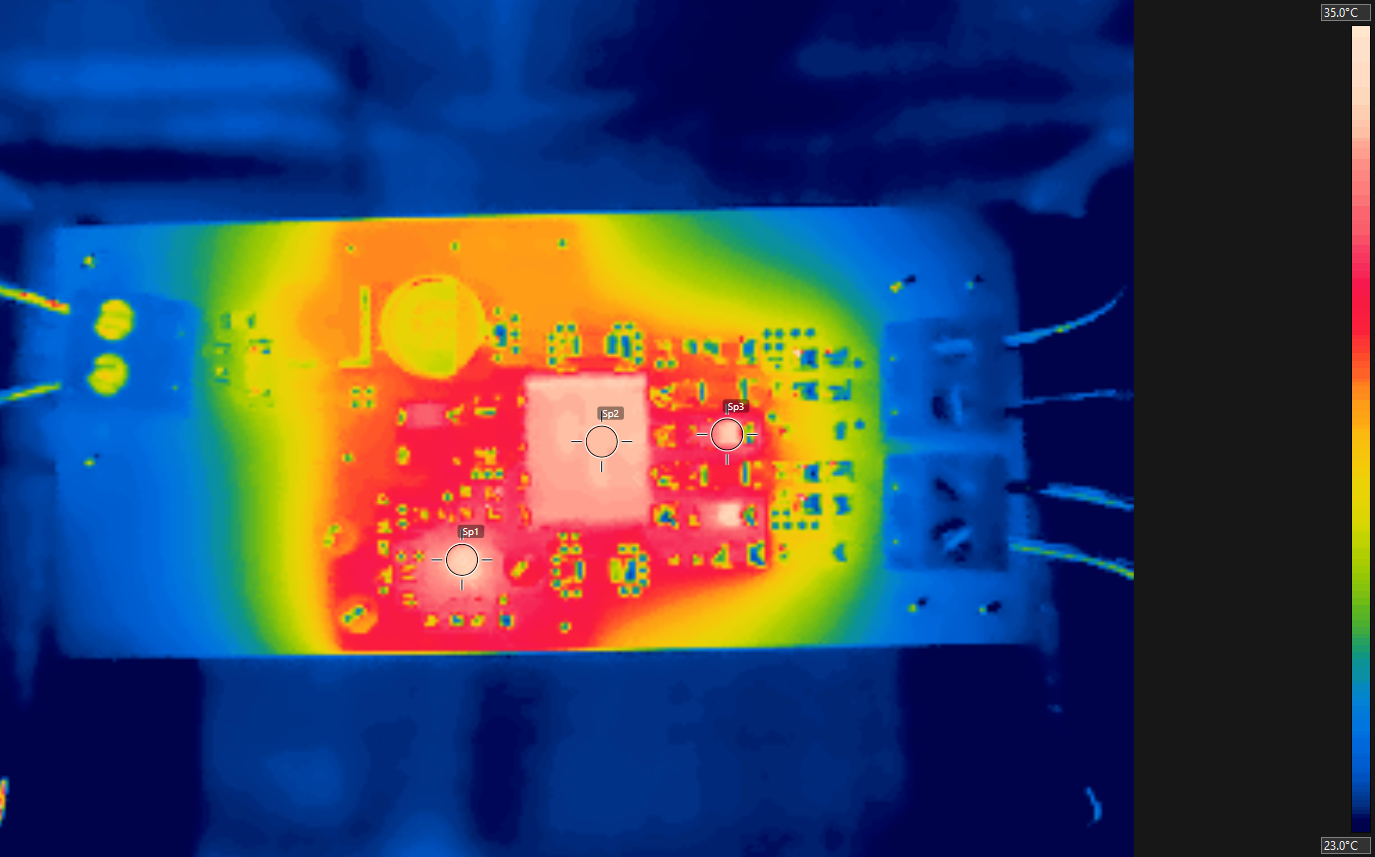
This thermal image shows the operating temperature of the top side of the board with 12-VDC input and both 15-V outputs loaded to 100 mA, while at room temperature and no air flow.
GUID-20210223-CA0I-NGHM-ZTR7-LXH8B5G8RK1Z-low.png

Measurement Location Temperature (C)
Sp1 33.8
Sp2 33.5
Sp3 33.7

Figure 3-1 Top Side Thermal Image