TIDT225 March 2021
3.2 Efficiency and Power Dissipation Graphs
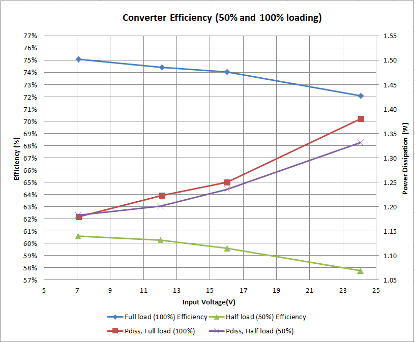
This data displays the efficiency and power dissipation of the converter at 50% and 100% of maximum output power at four different input voltages (7 V, 12 V, 16 V, and 24 V).
 Figure 3-3 Efficiency and Power
Dissipation Graph
Figure 3-3 Efficiency and Power
Dissipation GraphResistive loads were used as shown in the following table.
 Figure 3-4 Converter Load Resistance