TIDT226 April   2021


  1. 1Description
  2. 2Test Prerequisites
    1. 2.1 Voltage and Current Requirements
    2. 2.2 Required Equipment
  3. 3Testing and Results
    1. 3.1 Thermal Images
    2. 3.2 Efficiency and Power Dissipation Graph
    3. 3.3 Efficiency and Power Dissipation Data
    4. 3.4 Cross-Load Voltage Regulation
    5. 3.5 Voltage Regulation Graph
  4. 4Waveforms
    1. 4.1 Start-up Sequence
    2. 4.2 Switch Node
    3. 4.3 Output Voltage Ripple
    4. 4.4 Load Transients

Voltage Regulation Graph

This graph displays the total rectified secondary output voltage of the converter with a 24-VDC input voltage.
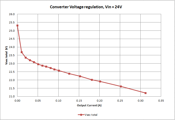
GUID-20210219-CA0I-FSQG-6C02-FHFNFHLJZZTS-low.png Figure 3-6 Converter Voltage Regulation for Vin of 24 V