TIDT226 April 2021
3.1 Thermal Images
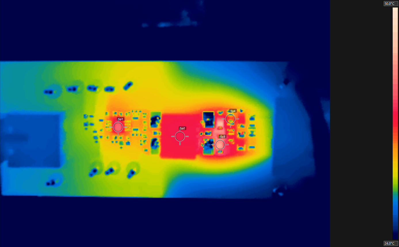
This thermal image shows the operating temperature
of the top side of the board with a 24-VDC input and the
+20 V and –4 V at 200-mA output at room temperature and no air flow.
 Figure 3-1 Top-Side Thermal Image With 200-mA
Load
Figure 3-1 Top-Side Thermal Image With 200-mA
Load| Measurement Location | Temperature (°C) |
|---|---|
| Sp1 | 41.7 |
| Sp2 | 38.9 |
| Sp3 | 44.6 |
| Sp4 | 36.4 |
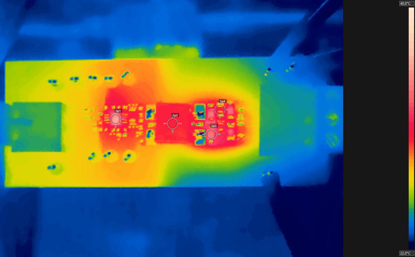
The following thermal image shows the operating temperature of the top side of the board with a 24-VDC input and the +20 V and –4 V at 100-mA output at room temperature and no air flow.
 Figure 3-2 Top-Side Thermal Image With 100-mA
Load
 | Measurement Location | Temperature (°C) |
|---|---|
| Sp1 | 36.3 |
| Sp2 | 30.4 |
| Sp3 | 34.4 |
| Sp4 | 30.7 |