TIDT239A April 2021 – July 2021
4.1 Switching
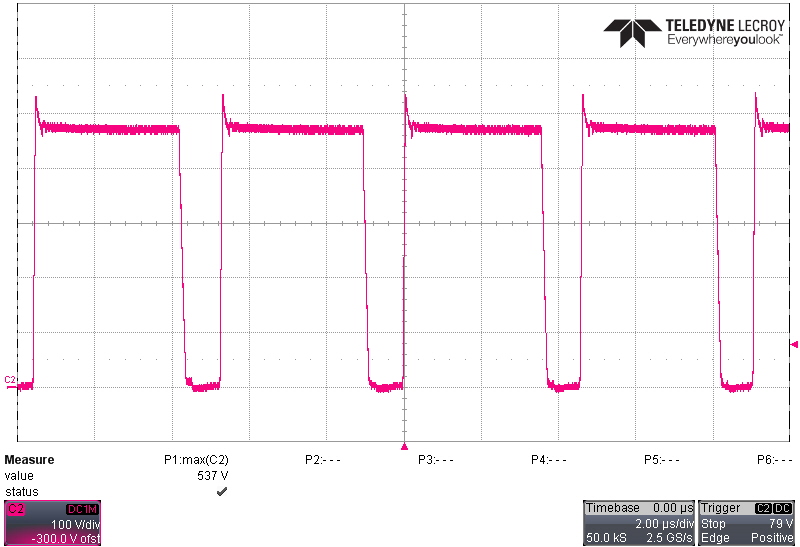
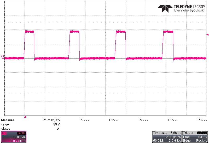
Switching behavior at 265 VAC, 50-Hz input is shown in the following figures. The highest voltage stress on both primary and secondary FETs occurs at highest input voltage and highest output voltage conditions. The voltage stress is highest on the synchronous rectifier (SR) FET during light loads when the UCC28782 disables ZVS operation to improve light load efficiency. At this condition, the non-ZVS results in a low-energy, high frequency spike on the drain of the SR FET.
 Figure 4-1 Primary FET (Q2) Drain-Source Voltage at 20 V,
3.25-A Output
 Figure 4-3 SR FET (Q5) Drain-Source Voltage at 20 V, 0-A
Output
 Figure 4-2 SR FET (Q5) Drain-Source Voltage at 20 V,
3.25-A Output