TIDT246 September   2021


  1. 1Description
  2. 2Test Prerequisites
    1. 2.1 Voltage and Current Requirements
    2. 2.2 Required Equipment
  3. 3Testing and Results
    1. 3.1 Efficiency and Power Dissipation Graphs
    2. 3.2 Efficiency and Power Dissipation Data
    3. 3.3 Thermal Performance
    4. 3.4 Bode Plot
    5. 3.5 Voltage Regulation
  4. 4Waveforms
    1. 4.1 Switching
    2. 4.2 Output Voltage Ripple
    3. 4.3 Start-up

Bode Plot

The loop stability of the boost converter is shown in the following plot. The plot was obtained with the LLC converter disabled and a resistive load applied across J2.
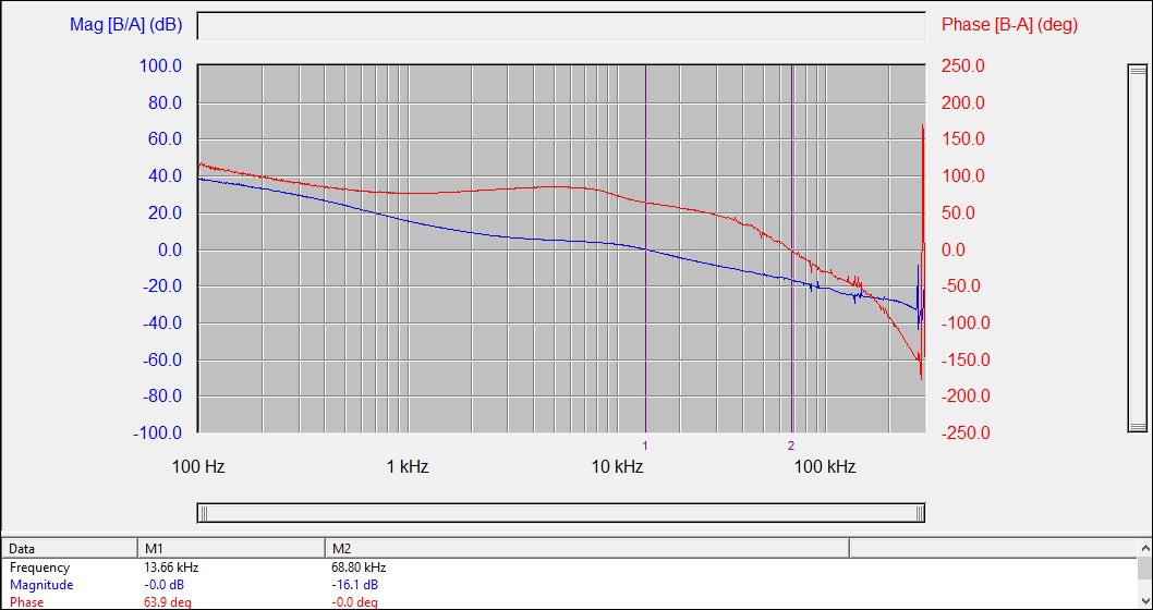
GUID-20210720-CA0I-SDVG-S7KK-RDF9JRDQXRJ9-low.jpgFigure 3-9 Loop Stability, 12 VIN, 250-mA Load